Mumbai. Friday, 12 June 2026
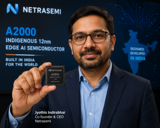
The global race for silicon dominance has officially entered a new chapter. In a definitive milestone for the nation’s tech landscape, Kerala-based fabless semiconductor startup Netrasemi successfully completed the initial post-silicon bring-up validation for its flagship AI system-on-chip (SoC), the A2000.
This breakthrough represents a massive cultural and economic shift. For decades, India has operated as the world’s premier back-office for chip design, hosting the engineering workforce for global tech giants while retaining none of the intellectual property (IP). By transitioning from a design service hub to a creator of proprietary chip products, India is cementing its role as a primary driver of the global computing engine—a critical transition highlighted in recent discussions on the next frontier for AI infrastructure investment.
The Reality Check: Where Was the A2000 Actually Made?
To truly appreciate this technical milestone, it is important to correct a common misconception: The A2000 was designed in India, but it was physically manufactured (fabricated) by Taiwan Semiconductor Manufacturing Company (TSMC) in Taiwan.
Netrasemi is a fabless chipmaker. This means their 91-member engineering powerhouse focuses entirely on building the intricate architectural blueprints and logic gates. Because building an advanced semiconductor fabrication facility (a “fab”) costs tens of billions of dollars and takes years to mature, outsourcing the physical printing of the silicon to TSMC’s established 12-nanometer (12nm) process node is standard global practice.
However, owning the Design IP—which includes Netrasemi’s proprietary Neural Processing Unit (NPU) and Vision Processing Unit (VPU)—is the highest-margin slice of the semiconductor business. The intellectual property and eventual profits stay directly within the Indian economy.
Why the 12nm Node is the Absolute “Sweet Spot”
While consumer smartphones race toward bleeding-edge 3nm or 2nm nodes, Netrasemi deliberately chose a 12nm architecture. This choice balances cost-efficiency with high-performance computing constraints.
The A2000 is engineered specifically for Edge AI applications. “Edge” computing refers to processing heavy data locally on the device itself—such as a security camera, a medical device, an industrial robot, or a defense drone—rather than transmitting that data to a distant cloud server.
[Raw Data: Video/Radar] ──> [On-Device 12nm A2000 SoC] ──> [Instant Local AI Inference]
                                                                 │
                                                    (No Cloud Latency / Ultra-Low Power)
By processing high-resolution video streams and vector data locally, the A2000 eliminates cloud latency, secures data from external interception, and fits perfectly within tight device power envelopes.
The Architecture of an Ecosystem: Beyond a Single Chip
Netrasemi’s individual success is a direct validation of India’s aggressive policy push. The startup was one of the first four firms selected by the Ministry of Electronics and Information Technology (MeitY) to receive financial backing under the ₹15 crore Design-Linked Incentive (DLI) scheme.
This milestone is also paving the way for a multi-tiered domestic hardware roadmap:
-
IoT Integration: Netrasemi is currently collaborating with the College of Engineering Trivandrum on the R1000, a low-power AI microcontroller built on an open-source RISC-V core for smart sensors.
-
Enterprise Scaling: The startup is already designing the A4000, an advanced “chiplet” architecture aimed at powering 500-TOPS enterprise AI servers by 2027.
-
The Fabrication Pipeline: While early validation chip runs are bound to overseas foundries, heavy capital is actively flowing into domestic infrastructure. Ground has already broken on major local manufacturing and advanced packaging projects, such as Tata Electronics’ upcoming assembly and fab lines in Dholera, Gujarat.
Challenges on the Horizon
Despite the incredible achievement of moving from digital blueprints to physical, functional silicon, major hurdles remain before the A2000 hits heavy commercial volume by mid-2027:
-
The Mask Set Cash Burn: Freezing a chip design into a permanent commercial “mask set” for mass production requires massive capital, often costing upwards of ₹50 to ₹100 crores. Continued institutional investment is vital.
-
Global Supply Chain Realities: Global investor trends have historically favored pure-play fabrication economies like Taiwan and South Korea, which can create temporary capital shifts away from diversified markets, as noted in assessments of India’s broader market resilience.
-
Local Adoption: True sovereignty relies on domestic original equipment manufacturers (OEMs) actively adopting local silicon over Western or East Asian alternatives.
Ultimately, the successful bring-up of India’s first indigenous 12nm AI system-on-chip proves that Indian deep-tech startups possess the engineering maturity to challenge global incumbents. The blueprint for a self-reliant digital economy is no longer just on paper—it is now etched into silicon.