

Mumbai. Monday, 13 July 2026
The global microelectronics landscape is undergoing a monumental architectural shift. Long recognized as the intellectual powerhouse behind international chip design, India is actively transitioning into a physical manufacturing powerhouse. Driven by a surge in domestic electronic consumption, rapid automotive electrification, and a collective global desire for supply chain diversification, industry consensus indicates that India’s semiconductor market is on a trajectory to expand to nearly $350 billion by 2035.
At the core of this industrial rebirth is the transition from localized software design to tangible, state-backed hardware ecosystems, supported directly by the evolution of the India Semiconductor Mission (ISM).
The Dynamic Growth Pillars: What is Fueling Chip Demand?
India is currently one of the largest single-nation consumers of electronic devices. However, the next decade of chip consumption will look drastically different than the past, moving away from low-complexity consumer chipsets toward specialized, high-performance silicon.
The AI and Data Center Boom: The rapid domestic expansion of hyperscale data centers requires specialized hardware architectures. Artificial intelligence workloads have permanently altered compute requirements, accelerating local demand for Graphics Processing Units (GPUs), high-bandwidth memory, advanced network routing fabric, and custom AI edge accelerators.
The Connected and Electric Vehicle (EV) Transition: Modern internal combustion engine vehicles rely on hundreds of microcontrollers, but an EV requires thousands. India’s burgeoning EV manufacturing sector relies heavily on power electronics, advanced battery management systems (BMS), motor controllers, and Advanced Driver Assistance Systems (ADAS).
Next-Generation Networks & Industry 4.0: The nationwide rollout of 5G infrastructure—and early development protocols for future 6G networks—demands massive deployments of high-frequency RF modules and network processors. Concurrently, manufacturing floors are integrating industrial robotics and Industrial Internet of Things (IIoT) sensors under the Industry 4.0 banner.
Policy Foundations: Creating Sustainable Manufacturing Momentum
To curb its heavy reliance on tech imports, the Government of India deployed a comprehensive capital support matrix designed to de-risk investments for international silicon giants and domestic conglomerates alike.
Key active pillars of this policy push include:
The India Semiconductor Mission (ISM 2.0): The central agency responsible for anchoring and processing multi-billion-dollar ecosystem proposals.
Production Linked Incentives (PLI) & Design Linked Incentives (DLI): Financial frameworks created to offset localized production scaling costs and subsidize domestic chip design start-ups.
Electronics Manufacturing Clusters (EMC): Dedicated industrial zones providing subsidized land, pre-built logistical channels, and communal effluent treatment facilities built specifically for cleanroom requirements.
The Active Assembly and Packaging Pipeline
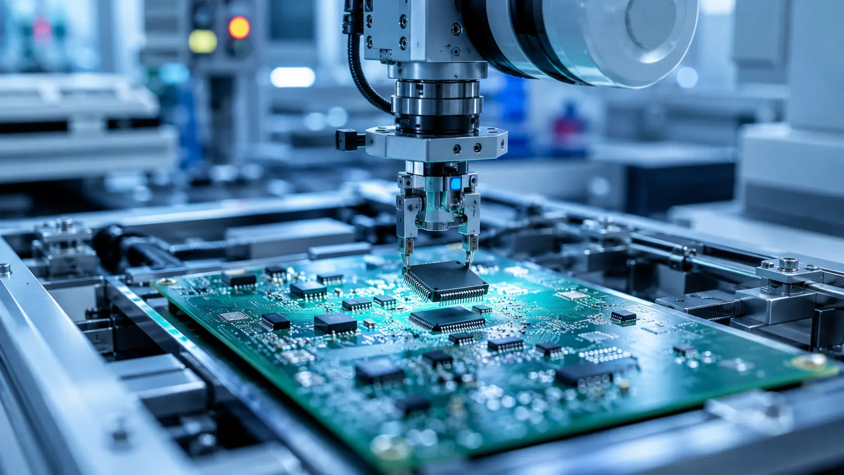
While advanced sub-nanometer logic wafer fabrication remains an intensive, long-term national objective, India has strategically prioritized midstream and downstream execution. Expanding Outsourced Semiconductor Assembly and Test (OSAT) and Assembly, Testing, Marking, and Packaging (ATMP) capacity allows the country to immediately integrate into the global electronics grid.
Major operational projects have materialized across key states:
Gujarat (Sanand & Dholera): Emerged as the primary operational hub, anchored by major packaging facilities like Micron Technology, CG Semi, and Kaynes Semicon starting commercial testing runs.
Compound Semiconductors: Investments are actively flowing into compound semiconductor fabs focusing on alternative materials like Gallium Nitride (GaN) and Silicon Carbide (SiC), critical for high-efficiency EV power electronics and display systems.
Navigating the Structural Bottlenecks Ahead
Despite historic capital infusions, establishing an independent microelectronics hub requires overcoming distinct infrastructural hurdles:
Sub-Fab Material Independence: The industry remains dependent on imported raw silicon wafers, high-purity chemicals, specialized gases, and extreme-precision photolithography tools.
Infrastructural Precision: Semiconductor facilities require absolute stability—even a micro-second drop in electricity grid voltage or a minor disruption in ultra-pure water supplies can ruin entire product runs.
The Talent Pivot: The country must successfully transition its massive base of software and verification talent into high-value manufacturing engineers, cleanroom operators, and process material experts.
Editorial Outlook: Setting the Global Standard
India’s long-term semiconductor goals go far beyond mere import substitution. By pairing its world-class, pre-existing chip design framework with expanding domestic OSAT capacities and multi-decade government subventions, the country is positioning itself as a reliable anchor for the global “China Plus One” supply chain strategy. By 2035, the Indian electronics landscape will not just consume technology—it will actively print, package, and supply it to the global digital economy.
Relevant Historical & Structural Context
For deeper research into the underlying technology, material supply chains, and industrial frameworks shaping these transformations, read the detailed sectoral briefings available on Matribhumi Samachar English:
To discover how local tech infrastructure is shifting toward advanced microchip architectures, review the analysis on The Rise of Hyderabad as a Global Hub for AI and Semiconductor Innovation.
Explore how advanced midstream packaging fills structural physical manufacturing gaps in Breaking Moore’s Law: Advanced Materials and Packaging Technologies.
Understand the physical foundation of the broader consumer hardware grid in The Blueprint of Modern Tech: Mapping the Complete Electronics Manufacturing Supply Chain.
Read about active localized downstream operations in India’s Silicon Leap: How the Sanand OSAT Facility Solidifies Domestic Electronics Manufacturing.
Frequently Asked Questions (FAQ)
Q1: Why is India focusing heavily on OSAT and ATMP facilities rather than advanced logic fabs?
Establishing advanced logic fabs requires immense capital investments and prolonged construction timelines. By prioritizing OSAT (Outsourced Semiconductor Assembly and Test) and ATMP facilities, India can establish immediate commercial footings, build local operational expertise, and integrate directly into global supply chains within shorter timelines.
Q2: What role does the “China Plus One” strategy play in India’s chip expansion?
Global electronics brands and semiconductor design firms seek to diversify their supply chains to guard against geopolitical disruptions and logistical shocks. India leverages this trend by combining its competitive production costs and government incentives with a vast engineering talent pool to attract global manufacturing partnerships.
Q3: How do electric vehicles (EVs) impact the demand for semiconductor microchips?
EVs depend fundamentally on semiconductors to govern high-voltage power distribution. They require chips for battery management systems, motor controllers, regenerative braking systems, and digital infotainment, resulting in significantly higher semiconductor content per vehicle compared to conventional internal combustion cars.
Disclaimer
Disclaimer: This article is prepared strictly for informational and educational purposes. The projections, market sizes, and project milestones are compiled based on contemporary industrial trends, government notifications, and market research available as of July 2026. Corporate investments, implementation timelines, and policy frameworks are subject to change based on global macroeconomic developments and changing institutional guidelines.
