Mumbai. Friday, 19 June 2026
The dream of transforming India into a dominant global silicon hub has officially shifted from executive boardrooms and policy proposals directly onto the factory floor. While initial blueprints mapping out the country’s high-tech destiny focused heavily on gathering intent, the physical realities of the India Semiconductor Mission 2.0 (ISM 2.0) have fundamentally reshaped the landscape. India is no longer just planning a tech ecosystem; it is actively constructing, packaging, and preparing to print silicon at a massive scale, positioning itself as an indispensable pillar of the worldwide high-tech supply chain.
For decades, India relied heavily on imported semiconductor chips used in smartphones, automobiles, consumer electronics, and defense systems. To reverse this import dependence, the Ministry of Electronics and Information Technology (MeitY) has driven immense structural investments, moving the nation away from acting as a “back-office” for global tech giants to retaining proprietary intellectual property (IP).
The Four-Phase Domestic Hardware Pipeline
To build complete technological sovereignty, the Indian hardware market operates across a precise, multi-tiered pipeline:
-
Phase 1: Upstream Chip Design & Proprietary IP – Leveraging the government’s Design Linked Incentive (DLI) scheme, domestic fabless startups create digital schematics. A prime example is Kerala-based semiconductor startup Netrasemi, which recently successfully completed the post-silicon validation for its flagship 12nm A2000 chip engineered specifically for Edge AI applications.
-
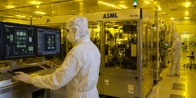
Phase 2: Front-End Fabrication (The Fab) – The complex chemical process of printing circuits onto raw silicon wafers. Tata Electronics’ upcoming mega-fab in Dholera, Gujarat—developed alongside Taiwan’s PSMC—is anchored here, targeting a massive 50,000 wafer starts per month.
-
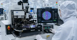
Phase 3: ATMP & OSAT Processing – Slicing raw silicon wafers into individual dies, packaging them securely, and testing them for performance. Commercial operations like Micron Technology in Sanand, Gujarat, and Kaynes Semicon have entered active commercial production, alongside Tata’s massive ₹27,000 crore Assembly, Testing, Marking, and Packaging (ATMP) unit in Jagiroad, Morigaon, Assam, which is built to handle up to 48 million chips per day.
-
Phase 4: Data Center & Industrial Integration – Routing finished hardware directly into indigenous automotive supply chains, telecommunications gear, and regional AI data infrastructure hubs.
High-Demand Careers and Core Skills in India’s Semiconductor Sector
As multi-billion-dollar semiconductor projects expand, they create a significant multiplier effect. Thousands of direct and indirect jobs are emerging across multiple technical disciplines. Students and professionals pursuing future-ready careers are focusing heavily on acquiring specialized skills:
| High-Demand Career Paths | Essential Technical Core & Skills |
| Semiconductor Design Engineer | VLSI Design, Chip Verification, Electronic Design Automation (EDA) Tools |
| Process & Equipment Engineer | Manufacturing Automation, Physical Prototyping, Cleanroom System Calibration |
| Packaging & Testing Specialist | Post-Silicon Validation, Stress Testing, Thermal Stability Tracking |
| AI Hardware Specialist | Custom Liquid-Cooled Architecture, Edge AI, Next-Gen Accelerator Design |
Beyond core engineering, extensive professional scopes are blooming in supply chain management, industrial automation, specialty chemical engineering, and facility management. Furthermore, regions like Jaipur are stepping up; through the Rajasthan Semiconductor Policy and institutions like MNIT Jaipur, localized semiconductor laboratories and virtual simulation platforms are training the foundational workforce required to fill these technical vacancies.
Emerging Frontiers: Next-Gen Gallium Nitride (GaN) Technology
While mainstream foundries are centering early market stability around traditional silicon processing nodes, advanced domestic R&D is pushing into next-generation alternative materials.
The integration of a state-of-the-art semiconductor testing laboratory at the Indian Institute of Science (IISc), Bengaluru—established by deep-tech startup AGNIT Semiconductors—focuses tightly on Gallium Nitride (GaN) validation. GaN technology outpaces traditional silicon in high-performance and high-frequency environments due to its distinct physical advantages:
-
Higher Power Efficiency: Drastically cuts energy loss in high-voltage operations.
-
Faster Switching Speeds: Crucial for processing massive data loads rapidly.
-
Superior Thermal Management: Chips remain cooler under intense loads, reducing bulky cooling needs.
This next-gen material is vital to powering high-frequency telecommunications architectures (5G and 6G) and maximizing electric vehicle (EV) onboard battery management networks.
Structural Challenges on the Horizon
Establishing an unshakeable semiconductor ecosystem requires navigating severe physical and economic constraints:
-
Pure Water and Power Grid Continuity: A typical commercial semiconductor fab consumes millions of gallons of water daily and demands absolute, uninterrupted clean electrical energy. A voltage fluctuation lasting even a fraction of a second can ruin an entire production batch of silicon wafers.
-
Extreme Capital Intensity: Upstream manufacturing equipment installation typically consumes roughly 65% of an entirely new facility’s capital layout, demanding sustained, synchronized financial support from both state subsidies and private funding.
By proactively addressing equipment manufacturing, raw specialty chemicals, and indigenous chip design simultaneously, India is building a resilient industrial shield against global supply chain vulnerabilities.
Frequently Asked Questions (FAQs)
1. What is the difference between Phase 2 (Fabrication) and Phase 3 (ATMP/OSAT)?
Phase 2 (Fabrication) involves printing highly intricate integrated circuits onto raw silicon wafers in multi-billion-dollar cleanrooms. Phase 3 (ATMP/OSAT) stands for Assembly, Testing, Marking, and Packaging. It is the phase where printed wafers are cut into individual dies, packaged safely into protective housings, and verified under intense stress conditions before going to market.
2. Where are the major semiconductor manufacturing hubs located in India?
While Gujarat (Dholera and Sanand) remains a critical anchor for large mega-fabs and testing facilities, advanced modules are geographically dispersed. Major units are scaling rapidly in Assam (Jagiroad, Morigaon), Odisha (Bhubaneswar), Uttar Pradesh (Jewar), and deep-tech design hubs in Rajasthan (Jaipur) and Karnataka (Bengaluru).
3. What role does Edge AI play in India’s semiconductor growth?
Edge AI chips allow hardware components in devices like smart cameras, drones, and medical equipment to process complex datasets locally. This removes dependency on distant cloud networks, eliminating operational latency and ensuring high data privacy.
External References
To discover a more detailed, investigative outlook on how active factory deployment, hardware pipelines, and localized testing facilities are reshaping the nation, read the complete field reporting directly from Matribhumi Samachar English:
-
Read the comprehensive report on Silicon Sovereign: How India Semiconductor Mission 2.0 is Transforming the Global Chip Landscape.
-
Explore active site developments via Silicon Sovereign: How India’s Semiconductor Push is Flipping the Switch to Active Production.
-
Understand the importance of native testing milestones through Silicon Sovereignty: How IISc’s New Testing Lab Plugs the Critical Gap in India Semiconductor Mission 2.0.
-
Analyze the hardware integration ecosystem at The Silicon and Steel Revolution: Inside India’s High-Tech Manufacturing Metamorphosis.
Disclaimer
This article is for informational and educational purposes only. The semiconductor market involves rapidly shifting technologies, immense corporate capital investments, and evolving state policies. Readers are advised to consult directly with official corporate announcements and updated ministerial notifications from MeitY for real-time commercial and financial evaluation.