

Hyderabad. Sunday, 12 July 2026
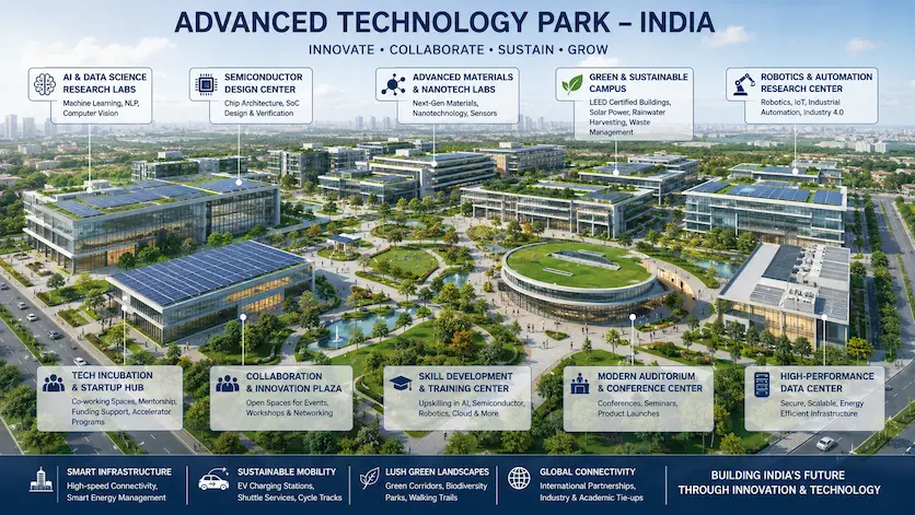
The landscape of Indian technology is shifting from high-volume software assembly toward specialized hardware, deep tech, and microchip architecture. Backed by proactive policy infrastructure, world-class research labs, and an increasingly sophisticated local talent network, Hyderabad has emerged as a key center anchoring India’s global tech aspirations.
By linking semiconductor design with heavy data center infrastructure and downstream electronics manufacturing, the capital of Telangana is engineering a completely self-contained, end-to-end technology value chain.
1. Government Framework and Policy Acceleration
The acceleration of Hyderabad’s deep-tech footprint relies heavily on aggressive, systemic governance. Rather than limiting public support to single-window corporate tax clearances, the Telangana state framework targets foundational layers of ecosystem scalability: advanced research capitalization, physical incubation networks, and localized digital infrastructure.
National-level initiatives like the India Semiconductor Mission (ISM 2.0) and the IndiaAI Mission act as powerful tailwinds, scaling municipal capacity to absorb foreign direct investments (FDI) and large-scale multinational research installations.
2. Unpacking the Integrated Value Chain
Hyderabad’s market strength lies in its refusal to compartmentalize hardware and software development. The city operates as an interconnected engine where different technological layers directly feed into and sustain one another.
+------------------------------------------------------------+
|                  SEMICONDUCTOR DESIGN                      |
| (Chip Architecture, SoC Development, EDA Verification Tools)|
+-----------------------------+------------------------------+
                              |
                     Feeds Architecture To
                              v
+------------------------------------------------------------+
|             ELECTRONICS & HARDWARE MFG                     |
|  (Advanced System Assembly, Aerospace & Defense Modules)   |
+-----------------------------+------------------------------+
                              |
                    Deploys Physical Systems
                              v
+------------------------------------------------------------+
|              DATA CENTRES & COMPUTE CLOUD                  |
|   (Local Sovereign AI Infrastructure, High-Density Racks)   |
+-----------------------------+------------------------------+
                              |
                    Powers High-Workload
                              v
+------------------------------------------------------------+
|                AI SOFTWARE APPLICATIONS                    |
| (Generative Models, Health Diagnostics, Automated Mobility)|
+------------------------------------------------------------+
Upstream: Advanced Semiconductor Design
While physical semiconductor fabrication plants (fabs) occupy massive headlines, the upstream phase—semiconductor chip design—demands an exceptionally high skill concentration. Hyderabad houses massive engineering design nodes focused entirely on:
System-on-Chip (SoC) Development: Consolidating computing modules onto single microchips for highly efficient processing.
Electronic Design Automation (EDA): Developing complex software frameworks to simulate, test, and refine microchip performance before manufacturing.
Firmware and Automotive Electronics: Building the core code that enables physical chips to control high-consequence automotive, aerospace, and medical systems.
Midstream: High-Density Data Infrastructure
Artificial intelligence demands extensive computation power. Large Language Models (LLMs) and complex deep-learning layers require reliable physical server clusters. Hyderabad has drawn significant private investment to expand high-density data centres. Supported by reliable power allocations and extensive regional fiber networks, these data campuses form a crucial infrastructure layer for sovereign AI processing hubs.
Downstream: Electronics Manufacturing and AI Verticals
The final phase converts hardware architectures and raw computational power into tangible consumer and industrial products. Local clusters integrate software design directly with specialized hardware production:
Medical Devices & Diagnostics: Deploying edge-AI algorithms inside physical diagnostic systems to improve patient identification metrics.
Smart Mobility & Industrial Automation: Fusing local Internet of Things (IoT) protocols with robotic systems to optimize supply networks.
Defense & Aerospace Systems: Assembling secure communication modules, radar equipment, and guidance computers within localized tech parks.
3. Academic Pipelines and the Startup Engine
A core competitive advantage driving this growth is the constant influx of specialized engineering talent. Local institutions function less like traditional academic settings and more like active incubators for high-value technologies. The International Institute of Information Technology, Hyderabad (IIIT-H)—which holds one of the country’s largest AI research footprints—works alongside facilities like the Indian School of Business (ISB) to blend technical engineering with commercial market scale.
This academic density directly supports extensive local incubation hubs. Venues like T-Hub allow early-stage deep-tech startups to build physical prototypes and connect with private venture capital networks, significantly shortening the path from lab concept to commercial product.
Frequently Asked Questions (FAQ)
What makes Hyderabad a primary center for semiconductor design?
Hyderabad features a dense concentration of specialized engineering talent focused on VLSI (Very Large Scale Integration), SoC frameworks, and Electronic Design Automation (EDA) tools. This pre-existing base allows global tech corporations to establish scalable engineering nodes efficiently.
How do data centres support the development of AI applications?
AI systems require extensive, continuous computation. Modern data infrastructure provides the underlying hardware, cooling capabilities, and high-speed data access needed to train, deploy, and scale deep-learning models.
How does academia collaborate with industries in Hyderabad?
Elite local institutions establish dedicated “Living Labs” and collaborative research agreements with enterprise tech brands. This setup allows students and research teams to address real-world industrial challenges using institutional facilities.
Disclaimer
This article is intended solely for informational, educational, and analytical purposes. It does not constitute investment, financial, or formal business consulting advice regarding real estate, stock allocations, or regional corporate relocation strategies.
Relevant External Resources
To further explore India’s current technological shift toward advanced hardware development, hardware engineering pipelines, and institutional breakthroughs, review these analytical overviews from Matribhumi Samachar:
For details on expanding technical career paths: The Silicon and AI Revolution: 10 High-Value Engineering Careers Exploding in India
For deep-tech infrastructure and university ecosystems: The Rise of Deep-Tech Innovation Hubs in Indian Universities
For details on localized collaborative hardware events: International Workshop on AI-Driven Semiconductor and Energy Efficient Hardware at T-Hub
