

Mumbai. Monday, 13 July 2026
The global electronics landscape is experiencing a profound architectural shift. While early structural blueprints for national technology strategies focused heavily on massive capital injections to build physical silicon manufacturing plants, real-world dynamics have proven that sustainable dominance requires a full-stack approach. Moving beyond the initial framework of attracting standalone fabrication plants, the Government of India is spearheading Semicon India 2.0. This next-generation policy evolution addresses the entire microchip value chain—from early-stage chemical formulation to advanced packaging systems.
By taking a holistic view of the ecosystem, the strategy aims to turn India from a powerhouse of software engineering into a highly resilient, globally integrated hardware hub.
The Strategic Leap: Moving Beyond Raw Fabrication
Building a modern semiconductor fabrication plant (or “fab”) is a massive technical achievement. However, a microchip is the result of a long, interconnected supply chain. The first phase of the India Semiconductor Mission (ISM) succeeded in anchoring multi-billion dollar manufacturing and testing facilities. Semicon India 2.0 expands on this by building out the structural pillars that support these massive cleanrooms.
A modern microchip passes through several critical stages before it ever enters a consumer device:
Upstream Research & IP Development: Creating new silicon architectures and patenting electronic design automation (EDA) tools.
The Design Core: Utilizing specialized engineers to construct application-specific integrated circuits (ASICs) and processors.
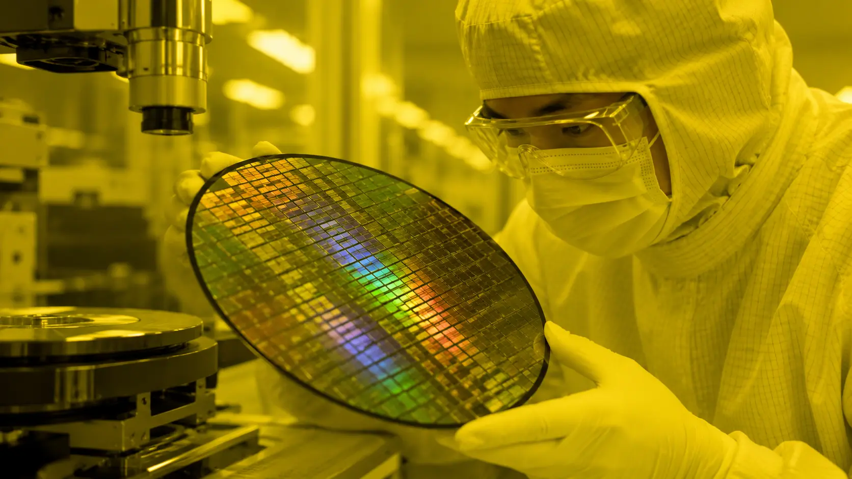
Wafer Fabrication: The high-precision chemical process of printing circuits onto raw silicon wafers.
Downstream Advanced Packaging (ATMP/OSAT): Assembly, testing, marking, and packaging the individual dies into finished products.
India already houses a massive talent network responsible for a substantial percentage of the world’s chip design work. The objective of the 2.0 framework is to commercialize this intelligence locally while strengthening upstream supply chains.
Strengthening the Indian Fabless and Design Ecosystem
A core pillar of Semicon India 2.0 is driving home-grown, startup-led chip innovation. Instead of relying solely on global firms to set up local engineering nodes, targeted incentives are pivoting to support indigenous processor architectures, custom artificial intelligence (AI) accelerators, automotive microcontrollers, and aerospace hardware.
This design focus directly complements India’s wider push into high-performance computing (HPC) and digital data centers. By nurturing small-to-medium design enterprises, the country can retain high-value intellectual property locally, creating a downstream multiplier effect for domestic device manufacturers.
Advanced Packaging: The New Performance Frontier
As traditional silicon fabrication approaches fundamental physical boundaries, physical performance upgrades no longer rely solely on carving smaller transistors onto a die. Advanced packaging has become the core driver of modern processing power.
Technologies like chiplet architectures, 2.5D/3D chip stacking, System-in-Package (SiP), and high-bandwidth memory (HBM) integration allow multiple specialized dies to work together seamlessly. Semicon India 2.0 heavily expands the policy framework for Assembly, Testing, Marking, and Packaging (ATMP) and Outsourced Semiconductor Assembly and Test (OSAT) units, positioning the country to capture this highly technical, high-margin piece of the global puzzle.
Localizing Materials and Equipment Upstream
A semiconductor factory cannot run without a steady stream of highly specialized industrial materials. The next phase of policy architecture targets the domestic production of high-purity chemicals, specialized industrial gases, silicon wafers, photoresists, and high-precision machinery components.
Localizing these upstream inputs removes severe vulnerabilities associated with international trade logistics and regional supply shocks. This ecosystem alignment is further supported by related high-tech supply chain programs, such as the ₹7,280-crore Rare Earth Permanent Magnet (REPM) Manufacturing Scheme, which aims to secure critical midstream processing for magnets used widely in automation robotics, defense systems, and cleanroom hardware.
Similarly, trade agreements like the India-Australia CECA 2026 are opening up reliable supply pipelines for critical minerals like lithium, cobalt, and rare earth elements, which are vital for powering next-generation electronic components and clean energy infrastructure.
Challenges and the Roadmap Ahead
Despite significant progress, the semiconductor roadmap involves navigating complex, long-term hurdles:
Sustained Capital Outlays: Fabs require ongoing, massive capital reinvestments to remain modern.
Talent Pipeline Scaling: Engineering curricula must continually evolve to train specialized cleanroom technicians and advanced packaging experts.
Upstream Gaps: While advanced design is robust, building local production capabilities for highly complex sub-components remains an uphill climb. For instance, as highlighted in current aerospace assessments like the Rise of Indigenous Defence Drones Report, high-end microcontrollers and guidance units still rely heavily on external silicon foundries.
Addressing these challenges will require ongoing collaboration between academic institutions, global technology vendors, and private venture funds. Rather than trying to compete purely on high-volume, low-margin legacy fabrication, the comprehensive strategy of Semicon India 2.0 builds a balanced, full-stack ecosystem. By weaving together design expertise, raw material security, and advanced packaging innovation, India is carving out a highly strategic, resilient position in the global technology footprint.
Frequently Asked Questions (FAQ)
Q1: What is the main difference between Semicon India 1.0 and 2.0?
Answer: While the first phase focused primarily on attracting physical manufacturing plants (fabs) and standard packaging facilities, Semicon India 2.0 broadens the scope to include the entire value chain, including advanced 3D packaging, raw materials processing, electronic design automation (EDA) tools, and localized IP development.
Q2: Why is advanced packaging emphasized in the next phase?
Answer: Traditional microchip scaling is hitting physical limits. Advanced packaging techniques (like 2.5D/3D stacking and chiplet architectures) allow multiple chips to be combined compactly, boosting processing speeds and reducing power consumption without needing to shrink the transistors further.
Q3: How do critical minerals and rare earths tie into the semiconductor mission?
Answer: Semiconductor cleanrooms, precision robotic handling tools, and downstream electronics all rely heavily on advanced materials and rare earth elements. Programs like the REPM scheme and agreements like the India-Australia CECA ensure that local factories have a steady, secure supply of these essential raw components.
Disclaimer: This article is intended solely for informational, educational, and analytical purposes. The details regarding the evolving policy frameworks, budget proposals, and international trade agreements are synthesized from current ministerial updates and public industrial statements available as of July 2026.
