

Mumbai. Friday, 17 July 2026
The global tech landscape is experiencing a massive shift, driven by a rapid artificial intelligence supercycle and urgent demands for hardware security. In response, India has officially crossed a major milestone in its evolution from a software outsourcing center into a physical, deep-tech manufacturing hub. Guided by the India Semiconductor Mission (ISM), the central government is preparing to roll out its highly anticipated Semicon 2.0 programme, establishing a progressive co-investment model to supercharge the country’s electronic and microchip value chain.
                    Traditional Grant Model (Semicon 1.0)
                    ├── One-time capital injection
                    └── High early-stage risk for private capital
                                      │
                                      ▼
                      Co-Investment Equity Model (Semicon 2.0)
                    ├── Pari-passu matching with top VC funds
                    └── Dynamic milestone-based capital scaling
The Co-Investment Shift: Equity Over Grants
The defining element of the Semicon 2.0 policy framework is the transition away from static, one-time capital subsidies toward an equity participation model. In traditional frameworks, deep-tech start-ups often struggled to cross the “commercialization gap”—the costly developmental phase where standard government grants run out before physical tape-outs or wafer validations are completed.
Under the new co-investment strategy, the government will invest pari-passu (on equal footing) alongside leading private Venture Capital (VC) firms. By directly acquiring equity stakes in high-potential deep-tech ventures, the state shares financial risks up front. The capital is disbursed through strict, milestone-based intervals tied directly to a startup’s technical and commercial milestones. This structure reduces early-stage exposure for private funds, attracting long-term institutional capital to the domestic chip sector.
To protect the flexibility of these emerging tech entities, the public equity stake is designed to remain below control thresholds, ensuring founders retain management autonomy. Crucially, the model features built-in buyback paths, allowing founders to repurchase the government’s equity once the venture achieves commercial profitability. This creates a self-sustaining cycle where returned state capital is continuously reinvested into the next wave of deep-tech startups.
Expanding the Value Chain: The Six Pillars of Focus
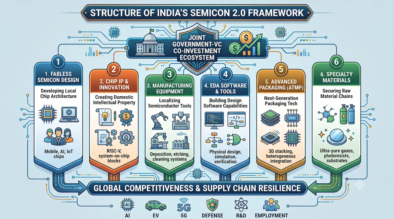
While the initial iteration of the India Semiconductor Mission concentrated on drawing massive, capital-heavy fabrication and assembly anchors, Semicon 2.0 expands horizontal and vertical depth across the entire ecosystem. The strategy focuses heavily on six critical segments:
Fabless Semiconductor Companies: Nurturing domestic architecture teams capable of building system-on-chips (SoCs) and original microcontrollers rather than merely executing outsourced design tasks.
Chip Design & Intellectual Property (IP): Providing specialized capital subsidies to protect and register indigenous electronic design assets globally.
Semicon Manufacturing Equipment: Securing downstream independence by building specialized precision tools, clean-room systems, and robotic assembly components locally.
Electronic Design Automation (EDA) Software: Reducing reliance on global proprietary design suites by supporting domestic open-source and specialized programming utilities.
Advanced Semiconductor Packaging: Channeling resources into next-generation packaging architectures, including 3D chip stacking, heterogeneous integration, and advanced chiplet configurations.
Specialty Materials & Components: Backing localized production of ultra-pure processing chemicals, electronic-grade specialty gases, and essential silicon substrates.
Securing Cross-Industry Technological Sovereignty
Expanding the semiconductor value chain directly reinforces India’s security and commercial capabilities across adjacent high-growth sectors. Localized silicon design and manufacturing insulate crucial domestic industries from volatile international supply disruptions, directly supporting:
Artificial Intelligence (AI): Powering domestic server architectures and data centers during an intense global AI hardware supercycle.
Electric Vehicles (EVs): Supplying high-power microcontroller units and power management integrated circuits (PMICs) crucial for automotive battery grids.
5G & 6G Infrastructure: Generating telecommunications processors and high-frequency RF modules to stabilize nationwide communication nodes.
Defense & Aerospace Systems: Ensuring reliable, untampered microchips for defense hardware, sovereign satellite arrays, and modern unmanned aerial vehicles (UAVs).
By moving past simple assembly toward full hardware ownership, India positions itself as an essential, high-value collaborator in the global electronics supply network, strengthening its long-term technology ecosystem.
Related Coverage from Matribhumi Samachar
To understand how these macro chip and industrial frameworks fit into India’s wider strategic networks, explore these detailed reviews:
Learn how localized components are strengthening defense platforms in The Rise of Indigenous Defence Drones: How India Is Engineering Its New Era of Military Self-Reliance.
Analyze how international critical material loops support hardware infrastructure via the India Australia CECA 2026 Briefing.
Track the primary baseline buildouts of the national electronics program in our previous guide, India Semiconductor Mission 2.0: The Rise of India’s High-Tech.
Review downstream component scaling initiatives under the India Extends ₹7,280-Crore Rare Earth Permanent Magnet (REPM) Scheme.
Frequently Asked Questions (FAQ)
Q1: How does the new co-investment framework differ from standard grant models?
A1: Traditional grant models offer a one-time financial subsidy that does not require repayment, leaving startups exposed if development timelines run long. The co-investment model functions as an equity partnership. The government matches private VC funds on a milestone-linked basis, sharing long-term risks while keeping the capital recyclable through structured founder buybacks.
Q2: What specific sub-sectors are prioritized under Semicon 2.0?
A2: The framework expands into six major pillars, including fabless chip design, specialized IP generation, Electronic Design Automation (EDA) tool development, chip packaging (OSAT/ATMP), upstream manufacturing machinery, and electronic-grade specialty chemicals.
Q3: Will the Indian government hold controlling stakes in the chip startups it funds?
A3: No. The co-investment model is designed to preserve operational agility. The government acts as a non-controlling financial partner, keeping its equity positions below majority levels to ensure private management and founders drive day-to-day operations.
Disclaimer
The information provided in this article regarding the proposed Semicon 2.0 framework is for general informational and educational purposes only. Policy provisions, fund allocations, and investment parameters reflect initial strategic proposals and remain subject to final regulatory notifications by the Ministry of Electronics and Information Technology (MeitY) and the India Semiconductor Mission.
