

Mumbai. Monday, 20 July 2026
India’s electronics manufacturing landscape is experiencing its most decisive transformation in decades. Historically anchored in low-margin final assembly, the country is executing a deliberate strategy to claim a deeper share of the global technology value chain—spanning component manufacturing, chip design, semiconductor fabrication, and advanced packaging.
Driven by aggressive sovereign policy frameworks, geopolitical realignments, and expanding domestic demand across automotive, defense, and AI infrastructure, India is positioning itself to shift permanently from “Made in India” to “Designed and Built in India”.
┌────────────────────────────────────────────────────────────────────────┐
│                   THE ELECTRONICS VALUE CHAIN LAYER                    │
├────────────────────────────────────────────────────────────────────────┤
│ 1. Raw Materials          ► Silicon, Specialty Gases, Rare Earths      │
│ 2. Electronic Components   ► PCBs, Capacitors, Connectors, Sensors     │
│ 3. Semiconductor Design    ► RISC-V, AI Accelerators, EDA & IP         │
│ 4. Chip Fabrication (Fab)  ► Legacy Nodes, Power & Compound Chips      │
│ 5. ATMP / OSAT Packaging   ► Advanced Packaging, Wafer Testing         │
│ 6. EMS & Integration       ► Sub-Assembly & System Board Level         │
│ 7. Finished Products       ► Smartphones, EVs, AI Servers, Defense     │
└────────────────────────────────────────────────────────────────────────┘
Deconstructing the Electronics Value Chain
To understand India’s trajectory, one must evaluate the individual layers of the electronics value chain and where the nation’s focus is rapidly shifting:
Upstream Raw Materials: Silicon, chemical reagents, rare earth elements, and industrial metals essential for base components.
Passive & Active Components: Multi-layer printed circuit boards (PCBs), capacitors, inductors, camera sensors, and battery management units.
Semiconductor Design: Architecture design, intellectual property (IP) creation, and Electronic Design Automation (EDA) tooling.
Semiconductor Fabrication: Front-end wafer fabrication across mature nodes, power devices, and compound materials.
ATMP / OSAT Operations: Assembly, testing, marking, and advanced packaging technologies.
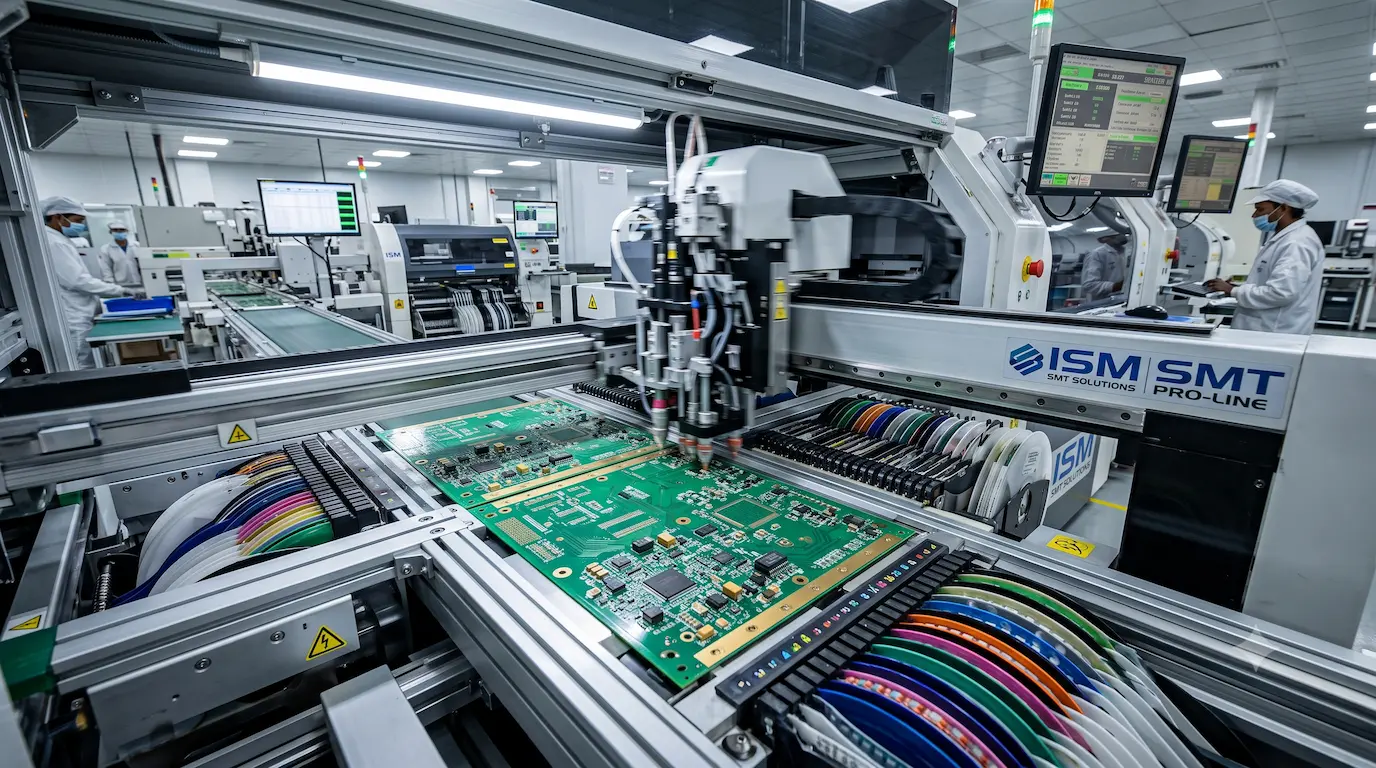
Electronics Manufacturing Services (EMS): System integration, surface-mount technology (SMT) lines, and structural testing.
End-Use Products: Consumer devices, electric vehicles (EVs), AI compute clusters, defense electronics, and 5G/6G telecom infrastructure.
1. Deep Componentization: Moving Beyond Assembly
While the conclusion of foundational incentives like the initial PLI schemes established India as the world’s second-largest smartphone producer, reliance on imported sub-assemblies remained a vulnerability. The nation’s policy focus has pivoted toward deep local component manufacturing.
Through dedicated schemes such as the Mobile Phone Manufacturing Scheme (MPMS) and broader component incentives, capital is flowing into high-value sub-assemblies:
Multi-layer PCBs and interconnects.
Display assemblies and camera modules.
Structural mechanical components and connectors.
High-density battery packs and battery management systems (BMS).
Power management integrated circuits (PMICs).
Increasing localized production directly lowers logistics costs, protects manufacturers from supply chain disruptions, and retains high economic value domestically.
2. Levering Design Dominance into Physical Silicon
For years, global semiconductor firms relied on engineering hubs in Bengaluru, Hyderabad, Noida, Pune, and Chennai for critical design work. Indian teams contribute directly to:
Custom RISC-V and ARM processor architectures.
Specialized AI accelerators and edge-compute processors.
Automotive microcontrollers and Advanced Driver Assistance Systems (ADAS).
RF transceiver modules, 5G networking chips, and power-efficient ICs.
Through Semicon 2.0 and design-linked incentives, the focus is translating this design dominance into physical domestic manufacturing and sovereign IP ownership.
3. The Semiconductor Push: Fabs, Packaging, and Materials
Transitioning from design to hardware requires high capital expenditure and sustained long-term commitment. Under the India Semiconductor Mission (ISM), physical infrastructure is taking shape across three primary fronts:
Mature-Node & Specialty Fabs: Focus on 28nm to 90nm nodes, along with Gallium Nitride (GaN) and Silicon Carbide (SiC) power semiconductors crucial for EVs, industrial drives, and defense.
Advanced OSAT / ATMP: Constructing domestic assembly, testing, and packaging capacity to capture immediate midstream value.
Upstream Raw Materials: Establishing domestic supply lines for high-purity chemicals, rare earths, and permanent magnets.
Demand Drivers Accelerating Growth
Demand across multiple high-tech verticals is driving adoption of domestically designed and manufactured components:
| Demand Sector | Critical Electronic Components & Chip Requirements |
| Automotive & EVs | Power electronics (SiC/GaN), BMS ICs, ADAS controllers, motor drive electronics |
| Artificial Intelligence | Edge AI silicon, high-speed memory packaging, data center power systems |
| Defense & Aerospace | Guidance navigation units (GNUs), transceiver modules, military-grade thermal arrays |
| Telecom & 5G/6G | Base station radio units, optical network processors, high-frequency RF modules |
Key Challenges Facing the Sector
Despite clear momentum, building a complete electronics ecosystem presents structural obstacles:
Capital Intensity: Advanced fabrication requires multi-billion-dollar investments with long payback periods.
Equipment Dependence: Global dependence on specialized lithography equipment, chemical vapor deposition systems, and EDA software.
Raw Material Security: Ensuring access to ultra-pure silicon and specialized gases.
Talent Upskilling: Rapidly scaling the workforce from pure design engineers into cleanroom, fab operations, and process integration experts.
Relevant Industry Coverage from Matribhumi Samachar
For further reading on policy blueprints, supply chain mappings, and deep-tech developments, explore these related articles on matribhumisamachar.com/en:
Frequently Asked Questions (FAQ)
Q1: How is India shifting from electronics assembly to full manufacturing?
India is incentivizing the domestic production of core sub-assemblies (such as multi-layer PCBs, camera modules, display assemblies, and power electronics) while expanding physical semiconductor fabrication and packaging (ATMP/OSAT) under initiatives like Semicon 2.0 and the MPMS scheme.
Q2: What role does semiconductor design play in India’s strategy?
India houses roughly 20% of the world’s chip design workforce. The current strategy focuses on leveraging this design expertise to create domestic intellectual property (IP), proprietary RISC-V architectures, and AI chips that can be physically produced in domestic fabs and packaging facilities.
Q3: Why are electric vehicles (EVs) vital for domestic electronics manufacturing?
Electric vehicles require significantly higher semiconductor and electronics content per unit compared to conventional vehicles—including battery management ICs, motor controllers, power electronics (SiC/GaN), and ADAS systems—creating sustained domestic demand for local components.
Disclaimer
This article is compiled for informational and educational purposes based on industry insights, government policy frameworks, and economic reporting. Future projections and policy outcomes depend on market dynamics, global supply chain conditions, and ongoing capital deployment.
