

New Delhi. Monday, 20 July 2026
India’s semiconductor ambitions have officially crossed a critical threshold. What began as a global design hub and expanded through initial investments in wafer fabrication plants and OSAT/ATMP (Outsourced Semiconductor Assembly and Test) units has now pivoted toward the most capital-intensive element of the microelectronics value chain: Semiconductor Fabrication Equipment.
A modern semiconductor fabrication plant (fab) relies on thousands of ultra-precision tools operating at nanometer scales. For India to establish long-term technological sovereignty, building domestic capabilities across tool manufacturing, subsystem assembly, clean-room robotics, and equipment control software has become a strategic priority under the country’s expanded Semicon 2.0 vision.
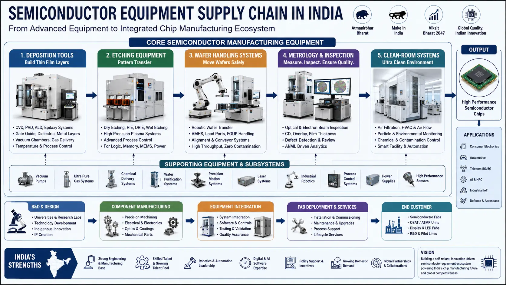
The Core Pillars of Semiconductor Equipment
Modern chip fabrication depends on specialized capital equipment working in absolute synchronization. Below is an overview of the key segments driving tool manufacturing:
┌─────────────────────────────────────────────────────────┐
│              CORE SEMICONDUCTOR EQUIPMENT               │
├───────────────┬───────────────┬───────────┬─────────────┤
│  Deposition   │    Etching    │  Handling │  Metrology  │
│ (CVD/PVD/ALD) │ (Plasma/DRIE) │  (Robotics│ & Inspection│
│               │               │   /FOUP)  │   (AI/CD)   │
└───────┬───────┴───────┬───────┴─────┬─────┴──────┬──────┘
        │               │             │            │
        └───────────────┴──────┬──────┴────────────┘
                               │
                ┌──────────────▼──────────────┐
                │ Clean-Room & Sub-assemblies │
                │ (Vacuum, Gas, Motion, MES)  │
                └─────────────────────────────┘
1. Deposition Equipment
Deposition tools add ultra-thin atomic layers onto silicon wafers to build gate oxides, dielectric layers, and metal interconnects.
Key Technologies: Chemical Vapor Deposition (CVD), Physical Vapor Deposition (PVD), Atomic Layer Deposition (ALD), and Epitaxy growth systems.
Localization Entry Points: High-vacuum chamber fabrication, mass flow controllers, precision temperature control units, and specialized gas delivery manifolds.
2. Etching Systems
Etching selectively removes material from the wafer surface to create circuit patterns.
Key Technologies: Dry plasma etching, Reactive Ion Etching (RIE), and Deep Reactive Ion Etching (DRIE).
Localization Entry Points: Radio Frequency (RF) generators, plasma chambers, and chemical-resistant fluid handling components.
3. Automated Wafer Handling & AMHS
To prevent contamination and maximize yield, modern fabs move silicon wafers via automated material handling systems (AMHS).
Key Components: Front Opening Unified Pod (FOUP) loaders, robotic transfer arms, vacuum load locks, and contactless conveyor networks.
Localization Entry Points: Industrial robotics, high-precision motion controls, and intelligent transport software.
4. Metrology & Inspection
Yield management relies on detecting sub-micron defects across millions of transistors.
Key Equipment: Optical inspection, Electron-beam (E-beam) defect scanners, Critical Dimension (CD) measurement tools, and surface profilometers.
Localization Entry Points: AI-driven computer vision models, defect-classification algorithms, digital twin software, and specialized optical lenses.
5. Clean-Room Facilities & Sub-systems
Fabs require Class 1 to Class 100 clean-room environments. Domestic opportunities are rapidly accelerating across air filtration systems, smart particle counters, ultra-pure water purification, and vacuum pump systems.
India’s Competitive Edge & Strategic Entry Points
While complete high-end lithography systems (such as EUV machines) remain controlled by a small group of global OEMs, India is carving out market share across high-value subsystems and software integration:
                     ┌───────────────────────────┐
                     │   INDIA'S ADVANTAGES      │
                     └─────────────┬─────────────┘
                                   │
         ┌─────────────────────────┼─────────────────────────┐
         │                         │                         │
┌────────▼────────┐       ┌────────▼────────┐       ┌────────▼────────┐
│   PRECISION     │       │   INDUSTRIAL    │       │   SOFTWARE &    │
│  ENGINEERING    │       │   AUTOMATION    │       │  AI INTEGRATION │
├─────────────────┤       ├─────────────────┤       ├─────────────────┤
│ CNC Machining,  │       │ Robotics, Motion│       │ MES, Predictive │
│ Aerospace, &    │       │ Control, Vision │       │ Maintenance,    │
│ Vacuum Systems  │       │ & PLCs          │       │ Digital Twins   │
└─────────────────┘       └─────────────────┘       └─────────────────┘
Precision Engineering: India’s defense, space (ISRO), and aerospace suppliers possess expertise in CNC machining, vacuum chambers, and specialized metallurgy.
Industrial Automation: Local automation firms are adapting motion controls, sensors, and PLC architecture for high-purity clean-room environments.
Software & AI Leadership: Modern tools require complex equipment management software (SEMI standards, SECS/GEM protocols), predictive maintenance suites, and real-time process simulation.
Strategic Roadmap for Startups & Industry
For startups and engineering companies entering the sector, building capability requires a phased approach:
Phase 1 (Immediate – Software & Analytics): Develop AI defect inspection software, digital twins, and fab automation software (MES).
Phase 2 (Medium Term – Sub-assemblies): Supply mass flow meters, ultra-pure gas valves, vacuum pumps, and robotic wafer loaders.
Phase 3 (Long Term – Specialized Capital Tools): Build legacy-node deposition/etching equipment, compound semiconductor processing tools, and specialized metrology instruments.
Frequently Asked Questions (FAQ)
What is the semiconductor equipment industry?
The semiconductor equipment industry comprises the specialized machinery, tools, sub-assemblies, and software systems used to manufacture, inspect, and package integrated circuits (chips) from raw silicon wafers.
Why is equipment manufacturing important for India’s semiconductor goals?
Capital equipment accounts for up to 70–80% of total fab investment. Localizing equipment, subsystems, and maintenance capabilities reduces import reliance, lowers operational expenditure, and establishes supply chain resilience.
What opportunities exist for Indian startups in chip equipment?
Startups can target high-value entry points including AI-powered defect detection, computer vision metrology, predictive maintenance platforms, digital twin simulations, ultra-high-purity gas delivery systems, and robotic handling units.
Does India intend to build lithography tools immediately?
No. Advanced EUV/DUV lithography tools represent the highest technical barrier in global manufacturing. India’s immediate focus under Semicon 2.0 centers on subsystems, metrology, automated handling, legacy tool refurbishing, and compound semiconductor tools.
Relevant Industry Links
For further reporting on India’s deep-tech manufacturing and semiconductor updates, visit:
Disclaimer
Disclaimer: The information presented in this article is compiled for educational and news reporting purposes based on industry trends, policy frameworks under the India Semiconductor Mission, and market developments as of 2026. Readers and investors are advised to conduct independent due diligence before making strategic or financial investments in the sector.
