

Mumbai. Monday, 20 July 2026
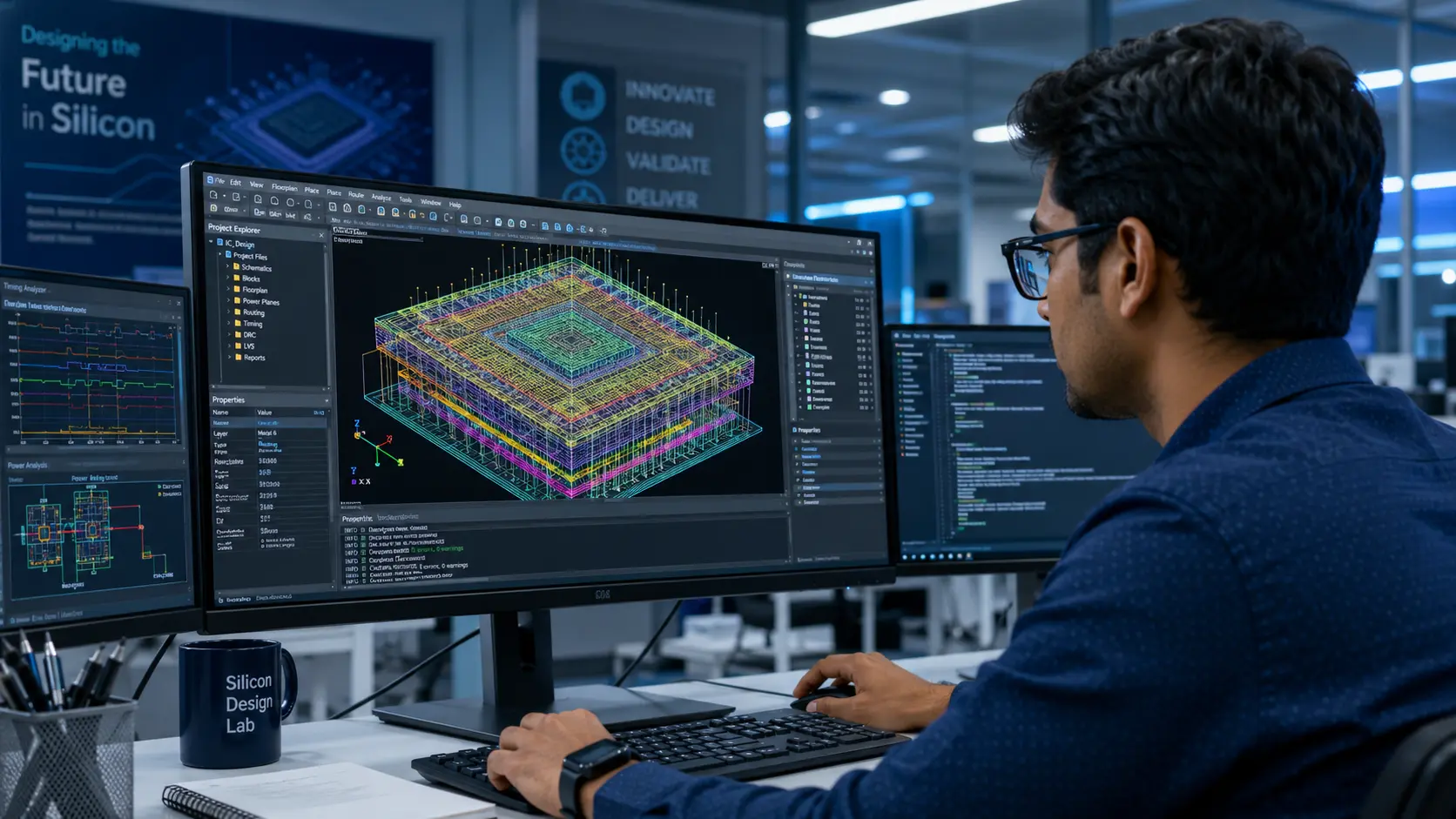
While global headlines frequently focus on multi-billion-dollar silicon fabrication plants (fabs), a quieter, highly strategic revolution is sweeping across India. Beyond physical cleanrooms and wafer fabrication, India is building an agile silicon ecosystem driven by over 105 fabless semiconductor startups.
From AI accelerators and automotive controllers to 5G RF hardware and defence-grade microprocessors, Indian engineering talent is pivoting from outsourcing services to building high-value, homegrown Intellectual Property (IP).
The Fabless Advantage: High IP, Lower Capital Intensity
Setting up a commercial semiconductor manufacturing facility (fab) requires upwards of $10 billion and years of infrastructure prep. In contrast, fabless chip design allows startups to innovate at a fraction of the cost.
Fabless firms focus entirely on:
Micro-architecture design & IP creation
Circuit verification and software stack integration
Logic simulation and physical layout tape-out
Once designs are finalized, manufacturing is outsourced to commercial foundries overseas or emerging domestic packaging hubs. This asset-light model yields higher profit margins and faster iteration cycles.
Key Industry Metric: India currently employs nearly 20% of the world’s semiconductor design workforce, housing R&D centres for global giants like Qualcomm, Intel, Nvidia, and Texas Instruments. The current fabless boom transitions this talent pool into IP owners.
Government Catalysts: DLI and C2S Schemes
Public policy and institutional support have been central to this momentum. Two anchor programs under the India Semiconductor Mission (ISM) are driving the shift:
1. Design Linked Incentive (DLI) Scheme
The DLI scheme provides financial incentives and infrastructure support covering up to 50% of eligible expenditure for:
ASIC & SoC Development: Custom silicon for AI, IoT, Telecom, and Automotive sectors.
Prototyping & Tape-out Costs: Reimbursing expensive multi-project wafer (MPW) runs at international foundries.
EDA Tool Access: Providing centralized access to enterprise Electronic Design Automation (EDA) software via national platforms like the ChipIN Centre.
2. Chips to Startup (C2S) Programme
Building the talent pipeline for the next decade, C2S focuses on academic-industry bridges:
100,000+ Enrolments across participating engineering hubs.
67,000+ Engineers Trained in VLSI, SoC architecture, and embedded systems.
305+ Academic Institutions actively participating in student tape-outs and reusable IP development.
Sector Breakdown: Where Indian Chips Are Heading
Rather than competing strictly in generic smartphone application processors, Indian chip startups are targeting specialized high-growth verticals:
| Target Market | Key Silicon Focus Areas | Real-World Application |
| AI & Edge Computing | On-device ML inference engines, neural processing units (NPUs) | Robotics, smart surveillance, edge vision |
| Automotive & EV | Battery Management System (BMS) ICs, ADAS controllers, motor drives | Electric vehicles, connected mobility |
| Telecom & 5G/6G | Sub-6GHz and mmWave RF transceivers, baseband processors | Cellular infrastructure, IoT gateways |
| Defence & Aerospace | Secure microcontrollers, radar DSPs, electronic warfare silicon | UAVs, satellite communications, tactical radios |
| Industrial IoT | Ultra-low-power MCUs, smart energy metering SoCs | Smart grids, factory automation |
Notable Indian Fabless Pioneers
Several startups have progressed beyond simulation models to physical tape-out, customer trials, and commercial deployment:
Mindgrove Technologies: Designing customizable, secure RISC-V-based SoCs for IoT and edge devices.
InCore Semiconductors: Developing modular RISC-V processor cores tailored for industrial and automotive applications.
Netrasemi: Specialized in vision AI chipsets for edge intelligence.
Agnit Semiconductors: Pioneering Gallium Nitride (GaN) power and RF semiconductor solutions.
Saankhya Labs & Signalchip: Building indigenous communication chipsets, SDRs, and 5G RF solutions.
Morphing Machines, Terminus Circuits, & Tattvam AI: Innovating in reconfigurable architectures, high-speed interfaces, and AI hardware acceleration.
Venture Funding & Commercial Traction
Investment momentum in the sector has accelerated rapidly:
24 semiconductor design projects approved under government frameworks with a combined project valuation near ₹900 Crore.
14 supported firms have successfully raised institutional venture capital.
Total private VC investment across Indian chip startups has surpassed ₹650 Crore, with multiple chips completing successful international tape-outs.
Remaining Challenges on the Horizon
Despite structural progress, key roadblocks persist:
Foundry Dependence: High reliance on overseas foundries (TSMC, GlobalFoundries) for advanced process nodes.
High Tape-out Expenses: Initial silicon runs remain capital-intensive for early-stage teams.
Packaging & OSAT Ecosystem: Developing local Assembly, Testing, Marking, and Packaging capacity to complete the supply chain.
Related Coverage from Matribhumi Samachar
For further reading on India’s deep-tech and semiconductor developments, explore these related reports:
India’s Silicon Boom: Top Semiconductor Career Opportunities and How to Prepare
Beyond the Fabs: Deconstructing India’s High-Stakes Upstream Semiconductor Race
India’s Chip Revolution: Mapping the 2026 Semiconductor Supply Chain Under Semicon 2.0
Frequently Asked Questions (FAQ)
What is a fabless semiconductor company?
A fabless semiconductor company designs, tests, and markets microchips and hardware intellectual property (IP) while outsourcing the actual manufacturing (fabrication) to specialized silicon foundries.
How does the DLI scheme support Indian chip startups?
The Design Linked Incentive (DLI) scheme offers financial reimbursements for prototyping, tape-outs, and IP creation, alongside providing centralized access to enterprise Electronic Design Automation (EDA) software.
Why is RISC-V popular among Indian semiconductor startups?
RISC-V is an open-standard instruction set architecture (ISA). It allows Indian design teams to build custom processors without paying high licensing fees required by proprietary architectures, fostering domestic innovation.
Disclaimer
This article is for informational and educational purposes only. Financial numbers, project approvals, and scheme details reflect reported metrics and government initiatives. Venture investment decisions should be made following independent due diligence.
