

Mumbai. Tuesday, 21 July 2026
When we talk about the world’s semiconductor revolution, the spotlight almost always falls on massive fabrication foundries (fabs)—giant, hyper-clean factories filled with multi-million-dollar lithography machines. But before a single nanometer of silicon can be etched inside a fab, an equally critical, high-stakes process takes place entirely on computer screens: Electronic Design Automation (EDA).
As India accelerates its hardware vision under the Semicon India 2.0 initiative backed by an expanded ₹1.27 lakh crore budget allocation, the nation is making a strategic pivot. India’s semiconductor strategy is no longer limited to bringing in physical fabs; it focuses heavily on capturing the highest-value upstream segment of the chip value chain—chip design and EDA infrastructure.
What Exactly is Electronic Design Automation (EDA)?
Think of modern semiconductor chips like ultra-dense cities built on a microscopic piece of silicon. A state-of-the-art AI processor or smartphone System-on-Chip (SoC) easily contains over 100 billion transistors, thousands of interconnected logic blocks, and complex power networks.
Designing something of this scale by hand is humanly impossible.
Electronic Design Automation (EDA) refers to a specialized suite of software algorithms, simulation environments, and hardware description platforms that enable engineers to plan, simulate, optimize, and verify microchips before manufacturing.
Without EDA tools, turning an architectural concept into a physical, functioning processor would take decades instead of months.
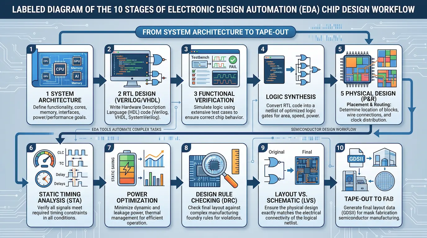
                  THE 10 STAGES OF CHIP DESIGN USING EDA

 [1. System Architecture] ──► [2. RTL Design (Verilog/VHDL)] ──► [3. Functional Verification]
                                                                        │
 [6. Static Timing Analysis] ◄── [5. Physical Design (Place/Route)] ◄── [4. Logic Synthesis]
            │
            ▼
 [7. Power Optimization] ──► [8. Design Rule Checking (DRC)] ──► [9. Layout vs. Schematic (LVS)]
                                                                        │
                                                                        ▼
                                                                [10. Tape-Out to Fab]
Step-by-Step: The 10 Major Stages of EDA Chip Design
System Architecture: Defining the high-level specs—CPU cores, GPU clusters, AI accelerators, and memory hierarchies.
RTL Design: Writing hardware description code using languages like Verilog, SystemVerilog, or VHDL.
Functional Verification: EDA simulators test millions of real-world scenarios to catch logic flaws before anything is etched in silicon.
Logic Synthesis: Translating human-readable RTL code into millions of interconnected logic gates optimized for speed and power.
Physical Design: Automated software maps component placement, signal routing, clock distribution, and power grids across metal layers.
Static Timing Analysis (STA): Checking that electrical signals reach every sub-circuit in exact picosecond windows.
Power & Thermal Optimization: Minimizing power leakage and heat buildup—critical for mobile devices and data center GPUs.
Design Rule Checking (DRC): Ensuring the layout strictly adheres to the physical manufacturing tolerances of the target foundry.
Layout Versus Schematic (LVS): Verifying that the final 3D physical layout precisely matches the original intended circuit diagram.
Tape-Out: Delivering the finalized digital mask files directly to the semiconductor manufacturing facility.
The Global EDA Titans
The global market for EDA software remains highly concentrated among a few specialized technology giants whose platforms are used by virtually every chip design team worldwide:
| Company | Core Expertise in EDA |
| Synopsys | Logic synthesis, AI-driven EDA tools (DSO.ai), digital design, IP libraries |
| Cadence Design Systems | Digital IC design, analog/mixed-signal verification, PCB design tools |
| Siemens EDA | Calibre physical verification, IC packaging, advanced PCB design |
| Ansys | Multi-physics simulation, electromagnetic & thermal analysis |
| Keysight Technologies | Radio Frequency (RF) simulation, high-speed test automation |
Why EDA is Central to India’s Semiconductor Sovereignity
India already houses roughly 20% of the global semiconductor design talent pool. Multinationals across major tech hubs—Bengaluru, Hyderabad, Noida, Pune, and Chennai—rely heavily on Indian design centers to taped-out cutting-edge chips.
However, historically, these engineers worked on intellectual property owned by foreign parent companies. Under India’s updated semiconductor strategy, the focus has shifted toward building indigenous fabless startups and creating domestic chip intellectual property (IP).
Key Policy Drivers Making EDA Accessible:
MeitY’s Design Linked Incentive (DLI) Scheme: Provides financial reimbursement and access to commercial EDA software suites for promising Indian fabless startups.
C-DAC’s ChipIN Centre: A centralized cloud platform offering over 300 universities and 100+ startups instant access to high-end EDA tool licenses from leading global vendors.
Chips-to-Startups (C2S) Programme: Focuses on training 85,000+ specialized engineers in advanced physical design, verification, and sub-5nm node workflows.
Key Challenges Facing the Indian EDA Landscape
Extremely High Licensing Costs: Full-suite enterprise EDA licenses can cost upwards of hundreds of thousands of dollars per engineer annually, presenting a steep entry barrier for independent startups.
Dependence on Foreign Software: Over 90% of global EDA tool revenue is held by US and European firms, making domestic tool creation a long-term strategic priority.
Advanced Node Complexity: Designing chips at 3nm, 2nm, or gate-all-around (GAA) architectures requires close integration with foundry-specific Process Design Kits (PDKs) and AI-assisted automation.
For a broader look at how these upstream software efforts connect with physical assembly and fab construction across the country, check out Matribhumi Samachar’s coverage on India’s 2026 Semiconductor Supply Chain as well as insights into India’s Silicon Boom and High-Tech Career Opportunities.
Frequently Asked Questions (FAQs)
1. What does EDA stand for in semiconductors?
EDA stands for Electronic Design Automation. It refers to specialized software applications used by hardware engineers to design, simulate, verify, and prepare integrated circuits (ICs) for manufacturing.
2. Can semiconductors be designed without EDA software?
No. Modern chips contain billions—sometimes over 100 billion—transistors on a piece of silicon the size of a fingernail. Manual design or verification at this micro-scale is mathematically impossible without automated EDA tools.
3. How is the Indian government helping startups access EDA tools?
Through the Ministry of Electronics and Information Technology (MeitY) and C-DAC’s ChipIN Centre, the government provides subsidized, cloud-based access to leading EDA suites (from Cadence, Synopsys, and Siemens) for eligible domestic fabless startups and academic institutions.
4. What are the most critical stages in EDA chip design?
While all 10 stages matter, Functional Verification (testing logic correctness) and Physical Design/Timing Analysis (ensuring component layout works within strict electrical limits) usually consume the largest share of engineering time.
Disclaimer
The information presented in this article is intended for educational and news reporting purposes only. Technical specifications, government scheme details (such as the India Semiconductor Mission and DLI scheme), and corporate tool offerings are subject to change based on official policy updates from the Ministry of Electronics and Information Technology (MeitY) and respective software providers.
