

Mumbai. Tuesday, 21 July 2026
As countries race to build resilient domestic semiconductor supply chains, popular focus naturally lands on massive fabrication plants (fabs), sleek chip architectures, and advanced 3D packaging. Yet, one of the most critical—and frequently overlooked—pillars of the global microchip value chain is testing and metrology.
Without extreme sub-nanometer measurement, rigorous defect inspection, and electrical validation, even the world’s most advanced fabrication plants cannot produce reliable microchips. For India, which is rapidly expanding its semiconductor ecosystem under the India Semiconductor Mission (ISM) and the Semicon 2.0 framework, mastering testing and metrology represents a game-changing strategic opportunity.
What Is Semiconductor Testing?
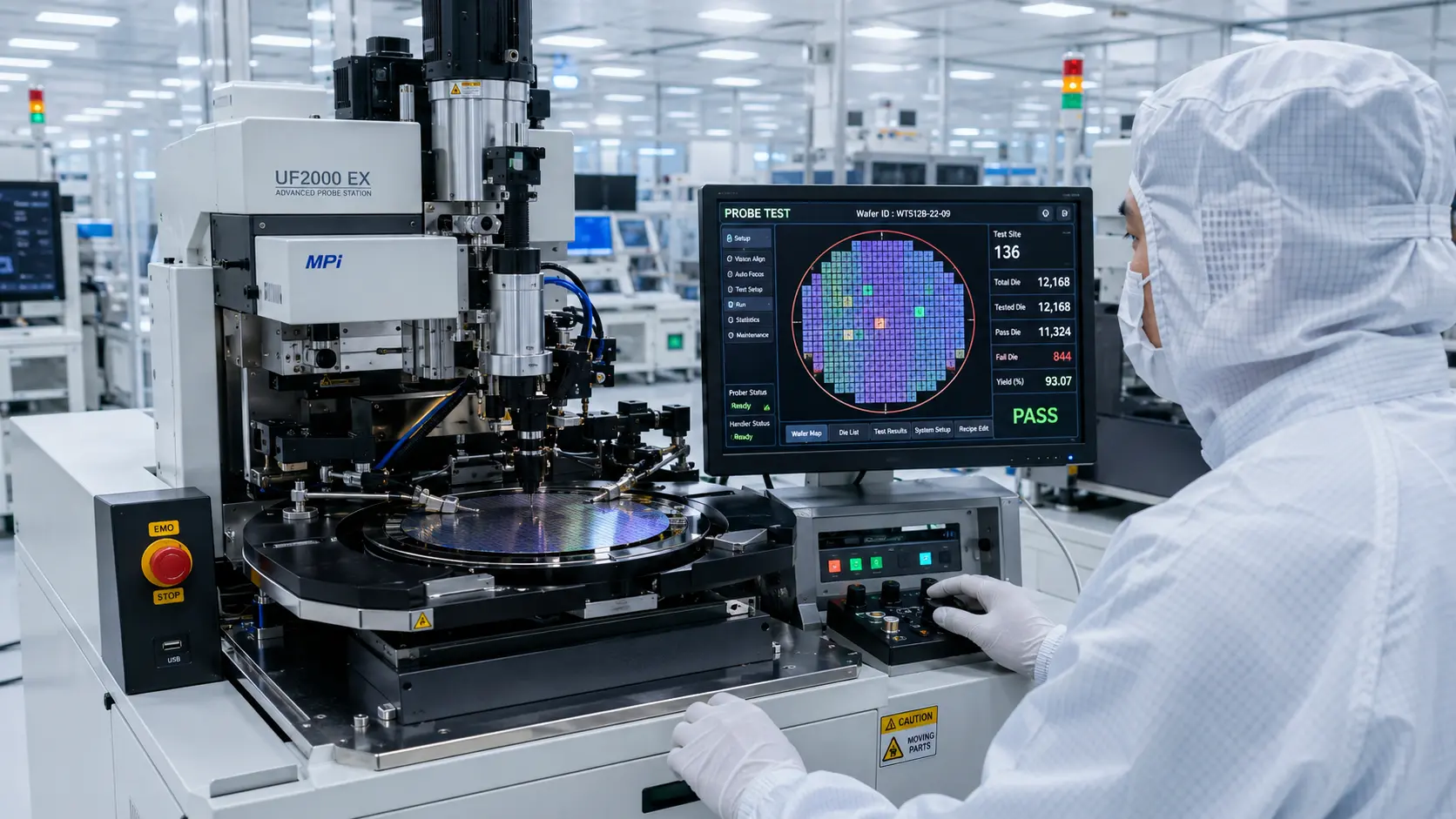
Semiconductor testing is the process of verifying that integrated circuits (ICs) operate as intended before they are shipped to customers. Because modern processors contain tens of billions of transistors etched into atomic-scale structures, a single microscopic flaw can destroy an entire chip’s functionality.
[Wafer-Level Probe] ──► [Post-Packaging Test] ──► [Burn-In & Stress Test] ──► [Final QA]
    (Detects bad dies)       (Logic/Memory check)      (Accelerated life testing)    (Market-ready)
Testing takes place in controlled phases throughout the manufacturing process:
Wafer-Level Electrical Testing (Wafer Probe): Probes assess dies directly on the silicon wafer to flag bad ones before expensive dicing and packaging occur.
Post-Packaging Functional Testing: Verifies that logic, signal integrity, and memory subsystems respond accurately once the die is housed inside its protective casing.
Parametric & Burn-In Testing: Exposes microchips to elevated voltages and extreme thermal stress to force early-life failures out before products reach high-reliability sectors like defense, aerospace, or automotive.
Final Quality Assurance: Ensures overall power efficiency, frequency targets, and thermal thresholds align with strict design specifications.
What Is Semiconductor Metrology?
While testing evaluates electrical performance, metrology is the science of measuring physical features with nanoscale precision. During fabrication, engineers must repeatedly measure critical dimensions (CD), thin-film thicknesses, pattern alignment (overlay accuracy), and surface topography across hundreds of processing steps.
+-------------------------------------------------------------------------------+
|                        Key Metrology Techniques                               |
+------------------------------------+------------------------------------------+
| Scanning Electron Microscopy (SEM) | Ultra-high resolution critical dimension |
|                                    | and failure analysis.                    |
+------------------------------------+------------------------------------------+
| Atomic Force Microscopy (AFM)      | Atomic-level 3D surface roughness        |
|                                    | mapping.                                 |
+------------------------------------+------------------------------------------+
| X-Ray Metrology & Ellipsometry     | Inspects hidden TSVs (Through-Silicon    |
|                                    | Vias) and thin-film layers.              |
+------------------------------------+------------------------------------------+
Without continuous metrology, small process deviations can slip through unnoticed, ruining entire silicon wafers and burning millions of dollars in material costs.
Yield Management: The Financial Core of Manufacturing
In semiconductor manufacturing, profit margins live and die by yield—the percentage of fully functioning chips produced on a single wafer.
The Math: If a $200\text{ nm}$ or $3\text{ nm}$ wafer yields only 60% usable chips, 40% of the expensive fabrication run becomes toxic electronic waste.
The Impact: Pushing yield from 70% to 85% or 90% to 95% saves chipmakers tens of millions of dollars annually while shortening time-to-market.
Metrology catches microscopic variations early, while automated testing isolates defective silicon before additional processing costs accumulate.
AI Transformation in Quality Control
Artificial intelligence has become essential for modern high-yield fabs. Machine learning algorithms process petabytes of high-resolution images generated by optical and SEM inspection systems in real time:
Automatic Defect Classification (ADC): AI vision models spot nanometer-scale line breaks or particle contamination faster and more accurately than human operators.
Predictive Maintenance: Analytics detect subtle calibration drifts in extreme ultraviolet (EUV) lithography tools before catastrophic downtime occurs.
Real-time Process Control: ML feedback loops automatically adjust chemical-mechanical planarization (CMP) parameters to maintain uniform film thickness across every wafer.
India’s Strategic Gateway: OSAT and ATMP Growth
India’s semiconductor roadmap wisely focuses not only on front-end silicon fabs but heavily on Assembly, Testing, Marking, and Packaging (ATMP) and Outsourced Semiconductor Assembly and Test (OSAT) facilities. Major investments—such as Tata Electronics’ OSAT facility in Morigaon, Assam, and Micron’s ATMP plant in Sanand, Gujarat—anchor this momentum.
Why Testing and Metrology Suit India’s Strengths:
Lower Capital Entry Barrier: While front-end silicon fabs cost upwards of $\$10\text{–}15\text{ billion}$, OSAT and ATMP plants require significantly lower upfront capital, enabling faster buildouts and quicker returns on investment.
Software-Hardware Synergy: India’s world-class software development pool provides a natural edge in Electronic Design Automation (EDA), test pattern generation (ATPG), and AI algorithm tuning for yield optimization.
Advanced Packaging Growth: As heterogenous integration (chiplets) and 3D stacking replace traditional monolithic dies, complex non-destructive testing (such as X-ray inspection for Through-Silicon Vias) becomes a high-value niche India can lead.
Industry Challenges & Future Horizon
As the semiconductor industry moves toward $2\text{ nm}$ process nodes, chiplet-based architectures, and high-bandwidth memory (HBM), inspection faces steep technical hurdles:
Massive Data Volumes: Inspection tools generate terabytes of raw data per hour, stretching data pipelines to their limits.
Complex 3D Structures: Inspecting stacked dies without physical destruction demands increasingly complex X-ray and acoustic imaging.
Specialized Talent Shortage: There remains a global shortage of metrology engineers who understand both physical nanoscale measurement and AI data pipelines.
Conclusion
Semiconductor testing and metrology may operate behind the scenes, but they form the true backbone of modern microchip manufacturing. Every reliable smartphone chip, AI accelerator, and electric vehicle controller depends on rigorous inspection before reaching consumers.
For India, developing world-class testing engineering, failure analysis labs, and AI inspection tools creates a key advantage, helping the country transition from a design talent hub into a global physical manufacturing leader.
Frequently Asked Questions (FAQ)
What is the difference between semiconductor testing and metrology?
Metrology measures physical dimensions, layer thickness, and surface structures during fabrication. Testing evaluates the electrical functionality, performance, and reliability of the chip before and after packaging.
What is OSAT, and why is it important for India?
OSAT stands for Outsourced Semiconductor Assembly and Test. OSAT facilities take fabricated silicon wafers, cut them into individual dies, package them, and run thorough functional tests. It allows India to build advanced manufacturing infrastructure quickly with lower capital risk compared to building multi-billion-dollar front-end fabs.
How does artificial intelligence improve semiconductor yield?
AI tools analyze massive inspection datasets to automatically identify nanoscale pattern defects, predict equipment wear, and continuously fine-tune manufacturing equipment to prevent yield drops.
Disclaimer
This article is published for informational and educational purposes. Semiconductor policy updates, corporate investments, and technology specifications reflect current data available under the India Semiconductor Mission (ISM) guidelines as of 2026. Readers are encouraged to consult official industry sources for investment or career decisions.
