

Mumbai. Wednesday, 22 July 2026
In a landmark move toward technological sovereignty and global supply chain leadership, the Government of India has officially entered the execution phase of India Semiconductor Mission (ISM) 2.0. Backed by a Union Cabinet approval of a fresh outlay totaling approximately ₹1.28 lakh crore ($13.25 billion), this phase represents the nation’s largest strategic push to date.
While the inaugural phase (ISM 1.0) laid the foundation by approving major manufacturing facilities across multiple states, ISM 2.0 shifts gears from standard manufacturing subsidies to establishing a fully integrated, self-sustaining semiconductor ecosystem.
What Happens Next: Implementation Roadmap
The roll-out of ISM 2.0 follows a structured, multi-stage roadmap intended to accelerate execution times and broaden industry participation:
Operational Guidelines Issuance: Immediate release of detailed framework criteria for global and domestic applicant eligibility.
Fresh Application Windows: Reopening proposals for silicon fabrication plants, ATMP/OSAT facilities, compound semiconductors, specialty materials, and equipment manufacturing.
Fast-Track Approvals: Streamlined single-window clearing mechanisms designed to expedite strategic investments.
Startup & Fabless Expansion: Enhanced financial incentives and Electronic Design Automation (EDA) access for chip design startups and fabless enterprises.
Infrastructure & Talent Support: Scaling state-of-the-art testing hubs, research facilities, and university-level talent programs.
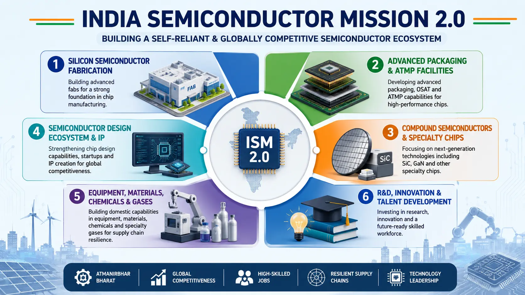
The Six Major Focus Area Pillars
ISM 2.0 moves beyond basic assembly to tackle every link in the semiconductor value chain:
                      ┌─────────────────────────────────────────┐
                      │    INDIA SEMICONDUCTOR MISSION 2.0      │
                      └────────────────────┬────────────────────┘
                                           │
         ┌──────────────────┬──────────────┴───────┬──────────────────┐
         │                  │                      │                  │
┌────────┴────────┐┌────────┴────────┐   ┌─────────┴────────┐┌─────────┴────────┐
│   Silicon Fab   ││ Advanced Packaging│   │ Compound & Special││  Design & IP  │
│   (Foundries)   ││   (ATMP/OSAT)   │   │   Semiconductors ││    Ecosystem     │
└─────────────────┘└─────────────────┘   └──────────────────┘└──────────────────┘
         │                                                            │
         └──────────────────────────┬─────────────────────────────────┘
                                    │
                         ┌──────────┴──────────┐
                         │ Equipment, Materials│
                         │   & R&D Workforce   │
                         └─────────────────────┘
Silicon Semiconductor Fabrication: Establishing commercial-grade foundries for leading-edge and mature nodes.
Advanced Packaging & ATMP/OSAT: Expanding high-density packaging, 3D heterogenous integration, and testing hubs.
Compound Semiconductors & Specialty Chips: Boosting Silicon Carbide (SiC), Gallium Nitride (GaN), and power electronics capabilities.
Semiconductor Design & Indigenous IP: Funding fabless startups to develop proprietary, domestically-owned intellectual property.
Equipment, Chemicals & Gases: Securing raw materials, ultra-pure specialty gases, and specialized tooling manufacturing.
Workforce & R&D: Deepening industry-led research hubs and training tens of thousands of specialized engineers.
Building Upon Phase 1 Successes
ISM 2.0 leverages the momentum created under the first phase:
| Metric / Program Area | Achievements Under ISM 1.0 | ISM 2.0 Targets |
| Approved Projects | 12 mega-projects across multiple states | Expanding coverage to raw material & equipment fabs |
| Pledged Investments | Exceeding ₹1.64 lakh crore ($17+ Billion) | Target to attract over ₹2.50 lakh crore in combined outlay |
| Design Support | 105+ startups/MSMEs equipped with EDA tools | Direct IP creation & expanded Design Linked Incentives (DLI) |
| Talent Pipeline | ~68,000 students trained across 315 universities | Industry-led training centers & advanced research labs |
Expected Economic Impact & Strategic Outlook
Industry analysts view ISM 2.0 as a critical turning point for India’s global trade positioning. The program aims to:
Reduce Import Reliance: Safeguard domestic industries against global chip shortages or geopolitical supply chain shocks.
Strengthen Key Sectors: Supply native chips to automotive, telecom (5G/6G), defense, healthcare, consumer electronics, and AI infrastructure.
Generate High-Value Employment: Create thousands of specialized engineering and advanced manufacturing jobs.
Elevate Global Status: Position India alongside established chip-manufacturing powerhouses as a reliable, resilient trade partner.
Frequently Asked Questions (FAQs)
What is the total budget for India Semiconductor Mission 2.0?
The Union Cabinet has approved a fresh outlay of approximately ₹1.28 lakh crore ($13.25 billion) for ISM 2.0.
How does ISM 2.0 differ from ISM 1.0?
While ISM 1.0 focused primarily on establishing foundational fabrication and packaging units, ISM 2.0 expands scope to cover raw material supply chains, equipment manufacturing, indigenous IP development, and dedicated workforce R&D centers.
Which industries will benefit most from ISM 2.0?
Automotive, telecommunications, artificial intelligence, defense, healthcare technology, and consumer electronics will directly benefit from local chip production and supply chain security.
Related News & Updates
For ongoing coverage, policy breakdowns, and national economic news, explore further updates at Matribhumi Samachar.
Disclaimer
This article is compiled based on official announcements, press releases, and secondary research regarding the India Semiconductor Mission (ISM) 2.0. Financial outlays, policy guidelines, and investment projections are subject to official government notifications and updates published periodically by the Ministry of Electronics and Information Technology (MeitY).
