

Bhopal. Friday, 24 July 2026
India’s ambition to establish itself as a global semiconductor powerhouse is reaching an exciting new phase. While Gujarat initially grabbed headlines as the primary hub for mega-fabs and large packaging plants, the nationwide chip footprint is expanding rapidly. In a major leap forward, Madhya Pradesh has officially joined India’s growing semiconductor map.
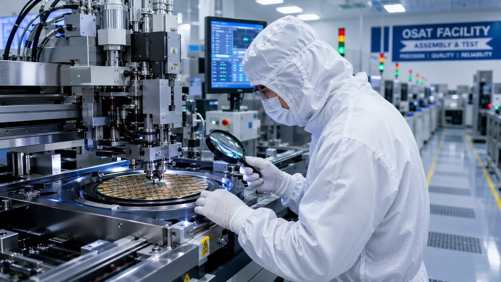
The state government has signed a proposed ₹6,200 crore investment agreement with Paras Semiconductors—a subsidiary of defense engineering firm Paras Defence & Space Technologies—to establish a state-of-the-art OSAT (Outsourced Semiconductor Assembly and Test) facility.
This milestone isn’t just a win for central India; it reflects a deliberate strategy under the India Semiconductor Mission (ISM) to create a resilient, geographically diversified high-tech manufacturing ecosystem across the country.
The Details: Inside MP’s High-Tech Breakthrough
The proposed greenfield facility will spread over approximately 50 acres along the Ujjain–Indore industrial corridor. The strategic placement provides seamless logistical connectivity across central India while drawing upon Madhya Pradesh’s growing industrial infrastructure.
Key Project Highlights:
Total Proposed Investment: ₹6,200 crore.
Employment Impact: Expected to create over 2,500 direct jobs, alongside thousands of skilled technical and indirect supply-chain roles.
Key Focus: Advanced integrated-circuit packaging, 2.5D and 3D heterogeneous packaging, hybrid bonding, chiplet integration, and wafer bumping.
Why OSAT is the Smart Play for India
Instead of immediately attempting to build multi-billion-dollar silicon wafer fabrication plants (fabs) in every state, focusing on OSAT and packaging builds essential capabilities faster and with optimized capital expenditure.
In the chip lifecycle, OSAT takes raw silicon wafers produced by foundries and converts them into protected, tested, and high-performing electronic components. As modern electronics shift toward specialized chiplets and complex 3D packaging, OSAT is where significant technological value is created.
┌─────────────────┐     ┌──────────────────────┐     ┌─────────────────────┐     ┌─────────────────────┐
│  1. Chip Design │ ──► │2. Wafer Fabrication  │ ──► │ 3. OSAT & Packaging │ ──► │4. System Integration│
│  (R&D Hubs)     │     │  (Foundry / Fabs)    │     │  (Testing / Bumping)│     │  (Finished Devices) │
└─────────────────┘     └──────────────────────┘     └─────────────────────┘     └─────────────────────┘
This facility will support critical domestic sectors including:
Defense & Aerospace: Radar platforms, electronic warfare, and secure satellite communications.
Automotive & EV: Powertrain management and sensor suites.
Artificial Intelligence & Telecommunications: High-density AI hardware, 5G/6G modules, and consumer electronics.
Why the Semiconductor Hub is Expanding Beyond Gujarat
Gujarat has undoubtedly laid strong foundations with pioneering projects like the Tata Semiconductor Plant in Dholera. However, concentrating an entire critical technology infrastructure in a single geographic cluster introduces supply chain risks.
India’s evolving strategy mirrors global chip leaders like Japan, Taiwan, and the US by distributing operations:
| Region / State | Core Focus & Industrial Advantage |
| Gujarat | Commercial wafer fabrication, large-scale assembly, port access. |
| Madhya Pradesh | Defense electronics, central freight corridors, advanced OSAT. |
| Karnataka | Chip design, R&D talent, software integration. |
| Assam | Large-scale assembly and testing facilities. |
| Tamil Nadu & UP | Electronics manufacturing services (EMS) and PCB component networks. |
The Strategic Defense Advantage
A key aspect of Paras Semiconductors’ involvement is its parent company’s heritage in defense and space engineering. For strategic defense hardware—such as optronics, missiles, and secure communications—trusted domestic packaging is just as critical as chip design.
Having an OSAT facility in central India ensures high reliability, tamper resistance, and supply security for sensitive defense applications, protecting vital systems from foreign supply-chain disruptions.
Challenges on the Horizon
While state-level incentives and MOUs mark a huge step forward, building a globally competitive chip ecosystem requires solving several remaining challenges:
Talent Pipeline: Training thousands of specialized technicians and VLSI packaging engineers.
Specialized Materials: Developing local supplies of semiconductor-grade ultra-pure chemicals and substrate materials.
Infrastructure Reliability: Ensuring zero-interruption, ultra-clean power and water utilities.
Frequently Asked Questions (FAQ)
What is an OSAT facility in semiconductor manufacturing?
OSAT stands for Outsourced Semiconductor Assembly and Test. It is the essential “back-end” phase of chip manufacturing where silicon wafers are cut into individual dies, enclosed in protective packaging, and tested for performance before being installed into devices.
Why did Paras Semiconductors choose the Ujjain–Indore corridor in MP?
The Ujjain–Indore region offers excellent multimodal logistics, competitive land acquisition costs, access to renewable energy, and central connectivity to manufacturing hubs across India.
How does this project support India’s defense sector?
Paras Semiconductors is backed by Paras Defence and Space Technologies. Domestic packaging allows India to manufacture trusted, tamper-proof chips required for military radars, secure communications, satellite electronics, and electronic warfare platforms without relying on foreign back-end facilities.
Disclaimer
The contents of this article are compiled for informational and educational purposes based on corporate announcements, state industrial development disclosures, and news reports. Project details, timelines, and regulatory approvals remain subject to final implementation agreements between the project developers and government authorities.
