Gandhinagar. Sunday, 14 June 2026
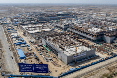
The dream of transforming India into a dominant global silicon hub has officially shifted from executive boardrooms and policy proposals directly onto the factory floor. At the heart of this high-tech revolution is the Tata Electronics-Powerchip Semiconductor Manufacturing Corporation (PSMC) chip fabrication plant in Dholera, Gujarat.
Widely regarded as India’s first commercial semiconductor wafer fabrication plant, this ₹91,000 crore facility is playing a pivotal role in reducing the country’s heavy dependence on imported chips while anchoring a new global electronics supply chain.
Major Construction Milestones Achieved in 2026
The Dholera semiconductor fabrication facility, approved under the Government of India’s aggressive India Semiconductor Mission (ISM) 2.0, has crossed massive engineering and infrastructure milestones. Large-scale civil works, cleanroom infrastructure, complex utility networks, and automated manufacturing support systems are advancing steadily at the Special Investment Region (SIR) site.
Developed in strategic partnership with Taiwan’s PSMC, the mega-fab is built for front-end fabrication—the complex chemical process of printing circuits onto raw silicon wafers. Once fully operational, the Dholera facility is targeting a massive production capacity of 50,000 wafer starts per month.
Strategic Importance: Pluggings Into the Global Hardware Pipeline
For decades, India operated primarily as a back-office for chip design, hosting the engineering workforce for global tech giants while retaining none of the core intellectual property (IP). The establishment of the Tata semiconductor plant in Dholera signifies a structural correction, moving India into Phase 2 of a completely indigenous, four-phase hardware pipeline:
-
Upstream Chip Design & Proprietary IP: Utilizing schemes like the Design Linked Incentive (DLI) to help local deep-tech startups retain IP.
-
Front-End Fabrication (The Fab): Pure silicon manufacturing, which is the primary focus of the Dholera mega-fab.
-
ATMP & OSAT Processing: Assembly, testing, and packaging. (Notably, this works in tandem with Tata’s parallel ₹27,000 crore OSAT unit breaking ground in Jagiroad, Morigaon, Assam).
-
Data Center & Industrial Integration: Routing finished hardware components directly into domestic automotive chains and expanding digital infrastructure.
[Phase 1: Local IP Design] ➔ [Phase 2: Dholera Fab Printing] ➔ [Phase 3: Assam OSAT Packaging]
➔ [Phase 4: Local AI Data Centers]
Advanced Manufacturing Capabilities and Node Selection
According to current project plans, the Dholera facility will initially focus on mature and proven semiconductor process nodes ranging from 28 nanometers (nm) to 110 nanometers.
While consumer smartphones often chase bleeding-edge 2nm or 3nm nodes, the 28nm–110nm range represents the absolute global “sweet spot” for market stability. These nodes remain in relentless demand for power-management integrated circuits, automotive microcontrollers, display drivers, and communication systems. This ensures immediate commercial viability and protects the facility from the extreme volatility often seen in ultra-advanced nodes.
Critical Infrastructure Challenges on the Rocky Road to Production
Building a world-class semiconductor ecosystem requires navigating intense engineering and administrative realities. Fabs are highly sensitive, resource-intensive environments where even minor external fluctuations cause catastrophic losses. Project stakeholders in Dholera are actively addressing two primary structural pillars:
-
Pure Water and Power Grid Continuity: A typical commercial semiconductor fab consumes millions of gallons of water daily and demands absolute, uninterrupted electrical energy. A voltage fluctuation lasting even a fraction of a second can ruin an entire production batch of silicon wafers.
-
Extreme Capital Intensity: Upstream manufacturing equipment installation typically consumes roughly 65% of a new facility’s capital layout. Sustaining this requires tightly coordinated financial tracks between private investments and state subsidies under ISM 2.0.
Production Timeline and Future Outlook
Equipment installation and cleanroom commissioning activities are accelerating rapidly. Initial test production runs and qualification cycles are actively targeted for late 2026, paving the way for commercial-scale manufacturing to ramp up systematically in 2027.
The successful commissioning of the Dholera facility will serve as an industrial catalyst. By addressing equipment manufacturing, raw specialty chemicals, and indigenous chip design simultaneously, India is ensuring that a global shipping freeze or external supply chain disruption won’t stall its high-tech future.
Relevant Links for Further Reading
For a deeper dive into how India’s technological infrastructure shield operates during global market shifts, and to explore parallel advancements in the hardware ecosystem, check out the complete investigative coverages from Matribhumi Samachar:
-
Read the full analysis on how the national chip push is altering global logistics: Silicon Sovereign: How India Semiconductor Mission 2.0 is Transforming the Global Chip Landscape.
-
Discover how domestic packaging feeds directly into data infrastructure: Silicon Sovereign: How India’s Semiconductor Push is Flipping the Switch to Active Production.
-
Learn about India’s breakthrough in proprietary AI system-on-chip hardware: From Blueprints to Silicon: How Netrasemi’s 12nm A2000 Chip Rewrites India’s Semiconductor Future.
-
Explore how other regional cities are backing this semiconductor workflow: Inside Jaipur’s Bold Leap into AI, Semiconductors, and Quantum Computing.
-
Understand the physical grid requirements sustaining these industrial assets: The Backbone of the Digital Revolution: Why India is the Next Frontier for AI Infrastructure Investment.