 Matribhumi Samachar English


Mumbai. Friday, 24 July 2026
If you have been keeping an eye on the tech world recently, you know that microchips—those tiny pieces of silicon that power everything from your smartphone to electric cars—have become the new oil. Nations across the globe are racing to secure their supply chains, and India is right at the center of this movement.
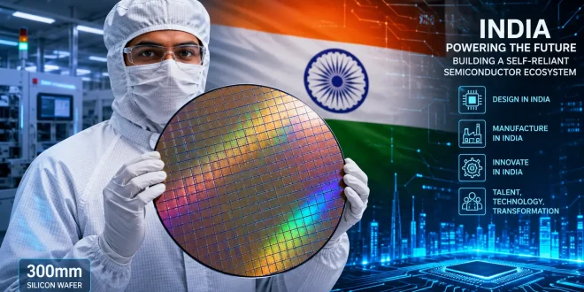
Through ambitious policy pushes like the India Semiconductor Mission (ISM) and the recently launched Semicon India 2.0, India is committing tens of billions of dollars to build a domestic ecosystem from scratch. But as commercial chips begin rolling off production lines in places like Sanand and Dholera, one big question stays on everyone’s mind: Can India replicate China’s rapid semiconductor rise?
To answer that, we have to look closely at what Beijing achieved over the last decade, where their state-led strategy hit walls, and how India’s unique playbook is forging a distinct—and perhaps more resilient—path forward.
🇨🇳 China’s Playbook: Massive Capital and Rapid Scale
Over the past decade, China treated semiconductor self-reliance as an urgent strategic emergency. Driven by international export restrictions, Beijing poured well over $100 billion into domestic chip development through its Big Fund initiatives, provincial subsidies, land grants, and low-interest financing.
China’s Big Wins:
Speed & Volume: Massive government backing allowed Chinese companies to build trailing-edge (mature) node capacity at record speeds.
Full Supply Chain Focus: Investments spanned silicon wafers, specialty gases, packaging, and etching equipment.
Talent Pipeline: Universities and government labs churned out thousands of specialized engineers annually.
Where China’s Model Stumbled
However, top-down funding without strict market discipline came with serious drawbacks:
-
Capital Inefficiency: Easy access to state money led to “ghost fabs,” duplicate projects, and overcapacity in basic nodes.
-
The Advanced Node Wall: Despite massive spending, cutting-edge sub-5nm manufacturing proved difficult to master without access to global, specialized lithography tools and IP.
-
Governance Bottlenecks: Lack of transparent oversight led to fund misallocation and delayed project delivery.
For deeper global tech comparisons, explore the Matribhumi Samachar Technology Desk.
🇮🇳 India’s Strategy: How Theory is Turning into Physical Reality in 2026
India is not trying to copy China’s playbook word for word—and that is a deliberate choice. Instead of attempting sub-5nm logic fabs right away or pumping unconstrained subsidies into unproven state entities, India’s India Semiconductor Mission focuses on smart sequencing and co-investment.
Under a generous 50% central fiscal support model (structured on a pari-passu basis where funds disburse as concrete is poured), India has attracted 12 major approved projects with total commitments crossing ₹1.64 lakh crore.
  Phase 1: Foundation (ISM 1.0)          Phase 2: Deep Ecosystem (Semicon 2.0)
┌─────────────────────────────────┐      ┌─────────────────────────────────┐
│ • Assembly & Packaging (OSAT)   │ ───► │ • Equipment & Material Fabs     │
│ • Mature Node Fabs (28nm+)      │      │ • Domestic Design IP & Startups │
│ • Anchor Units (Micron, Tata)   │      │ • Specialized Chemicals & Gases │
└─────────────────────────────────┘      └─────────────────────────────────┘
The 2026 Status Check:
-
Assembly & Packaging First (OSAT/ATMP): Commercial output is already live! Micron’s assembly plant in Sanand, Gujarat, along with facilities from Kaynes Semicon and CG Semi, are active, delivering finished modules to global buyers.
-
Front-End Fab Progress: Construction on Tata Electronics’ ₹91,000 crore mega-fab in Dholera (in partnership with Taiwan’s PSMC) is progressing to produce 28nm to 65nm chips for automotive and industrial markets.
-
Semicon 2.0 Expansion: The Cabinet’s approval of Semicon India 2.0 (with an outlay of ₹1.27 lakh crore) shifts focus to equipment manufacturing, specialty chemicals, cleanroom infrastructure, and domestic chip design IP.
For local policy updates, visit Matribhumi Samachar Business Section or read our latest report on the Semicon India 2.0 Cabinet Approval.
📊 Comparison at a Glance: China vs. India
| Metric / Dimension | China’s Strategy | India’s Evolving Playbook |
| Funding Mechanism | Top-down state investment ($100B+) | Co-funding model (50% central support on pari-passu terms) |
| Initial Priority | Broad import substitution & front-end fabs | OSAT/Packaging & mature-node logic (28nm+) |
| Design Strength | Growing, but historically equipment-reliant | World-leading design base (~20% of global IC design workforce) |
| Global Alignment | Forced self-reliance under export restrictions | Integration as a “Trusted Partner” (US, EU, Japan, Taiwan) |
| Ecosystem Goal | Rapid self-sufficiency | Resilient, market-driven integration in global value chains |
💡 Key Lessons India Must Follow to Win
-
Build the Upstream Stack: A fab cannot survive without gas suppliers, ultra-pure water, specialty chemicals, and testing facilities nearby.
-
Prioritize Talent Conversion: India already hosts 20% of the world’s chip design engineers. The challenge is training thousands of hands-on process and cleanroom engineers.
-
Focus on Commercial Off-Take: Ensure local demand from India’s surging $200B+ electronics and EV manufacturing sectors absorbs domestic chip output.
-
Maintain Long-Term Policy Stability: Semiconductor facilities take 3–5 years to build and decades to yield returns. Consistent policy across state and central levels is crucial.
💬 The Final Takeaway
India does not need to duplicate China’s exact path to become a semiconductor powerhouse. Where China relied on sheer state volume, India can succeed through market-aligned funding, strategic international partnerships, and unmatched design expertise.
By mastering packaging, scaling mature nodes, and expanding into equipment and design IP under Semicon 2.0, India is laying the foundation for a durable, world-class chip ecosystem.
Stay updated with national technological breakthroughs on the Matribhumi Samachar News Hub.
❓ Frequently Asked Questions (FAQ)
1. What is the India Semiconductor Mission (ISM)?
The India Semiconductor Mission (ISM) is a specialized administrative and financial initiative under the Ministry of Electronics and Information Technology (MeitY). It provides fiscal incentives and policy support to companies setting up chip fabs, packaging units (OSAT/ATMP), and design centers in India.
2. Why is India focusing on mature nodes (28nm+) instead of 2nm/3nm chips?
Mature nodes (28nm to 90nm) power over 70% of global semiconductor demand, including electric vehicles, microcontrollers, medical equipment, and consumer appliances. They are commercially viable, less capital-prohibitive, and align with India’s immediate electronics manufacturing needs.
3. How does Semicon 2.0 differ from the initial Semicon India scheme?
While Semicon 1.0 focused heavily on attracting anchor facilities like OSAT plants and logic fabs, Semicon 2.0 expands support across the wider supply chain—targeting semiconductor manufacturing equipment, specialty raw materials, cleanrooms, and indigenous IP creation.
4. Is India already producing microchips commercially?
Yes! As of 2026, assembly, testing, and packaging (ATMP/OSAT) facilities—including Micron’s plant in Sanand and Kaynes Semicon—have commenced commercial production, shipping packaged memory and logic chips to domestic and global customers.
⚠️ Editorial Disclaimer
The information presented in this article is compiled from official government releases, industry reports, and verified news sources as of July 2026. Views and market projections expressed herein are for educational and informational purposes only and do not constitute financial or investment advice. Readers are advised to consult certified industry analysts before making commercial decisions.