

Bengaluru.
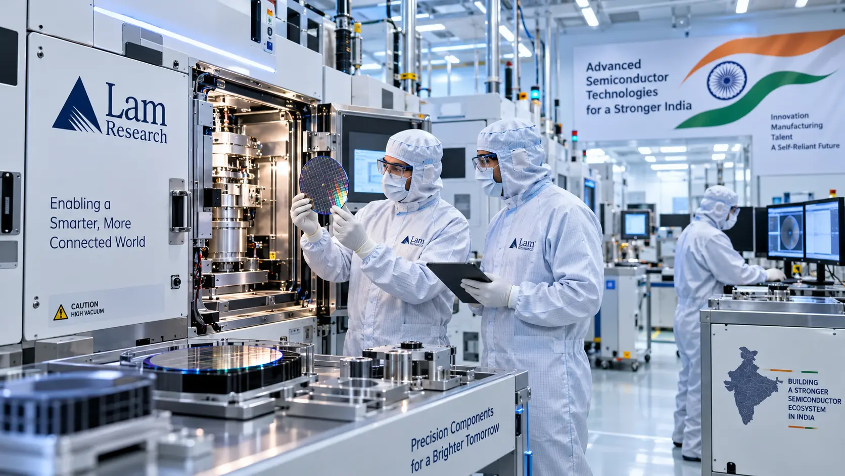
US-based semiconductor equipment giant Lam Research Corporation has announced plans to invest approximately ₹10,000 crore (~$1.2 billion) in India over the coming years. The move establishes the company’s first silicon component manufacturing facility in India while expanding its engineering and research and development (R&D) operations in Bengaluru.
The expansion marks a transition for India’s technology sector—moving beyond software engineering and chip design into high-precision industrial manufacturing for global semiconductor supply chains.
Inside the Investment: Silicon Components and R&D
The ₹10,000 crore outlay focuses on two operational pillars:
- Silicon Component Manufacturing Facility: The plant will execute vertically integrated processes, including silicon ingot production and precision machining. These ultra-high-purity components are critical inside modern plasma etching and chemical vapor deposition (CVD) tools.
- Expansion of Bengaluru R&D Center: Lam Research will grow its India Center for Engineering in Bengaluru, which already contributes to global product design, simulation, hardware testing, and software validation for next-generation chip nodes.
+-----------------------------------------------------------------------+
|                 LAM RESEARCH INDIA EXPANSION PILLARS                  |
+-----------------------------------------------------------------------+
|  1. Silicon Manufacturing       |  2. Engineering & R&D Expansion     |
|     - Silicon Ingot Production  |     - Next-Gen Node Architecture      |
|     - Precision Component Tools |     - Process Simulation & Testing    |
|     - Upstream Equipment Parts  |     - Software & Hardware Engineering |
+-----------------------------------------------------------------------+
Why Silicon Components Matter in Wafer Fabrication
Inside semiconductor fabrication plants (fabs), silicon components face corrosive plasma gases, extreme heat, and sub-nanometer tolerances.
- Purity & Contamination Control: Impurities inside processing chambers can destroy wafer yields. Manufacturing components from semiconductor-grade silicon ensures material compatibility.
- Thermal & Chemical Durability: Components must withstand constant plasma exposure without degrading, requiring specialized precision manufacturing techniques.
- Supply Chain Resilience: Localizing component production reduces global supply delays for equipment OEMs and fab operators.
Workforce Development & Industry Impact
To support this expansion, Lam Research continues its workforce collaboration with the India Semiconductor Mission (ISM) and academic institutions like the Indian Institute of Science (IISc). Through its Semiverse Solutions virtual platform, the program aims to train up to 60,000 engineering students in semiconductor fabrication and equipment management.
The investment also creates commercial opportunities for local Indian suppliers specializing in high-purity industrial gases, specialty chemicals, precision machining, and industrial automation.
Relevant Links & Sources
- Read full tech industry coverage at Matribhumi Samachar English.
- Explore background insights on Matribhumi Samachar Business News.
Frequently Asked Questions (FAQ)
Q1: What is Lam Research planning to invest in India?
Lam Research plans to invest approximately ₹10,000 crore to build a silicon component manufacturing facility and expand its advanced R&D center in Bengaluru.
Q2: What are silicon components used for in semiconductor manufacturing?
Silicon components are high-purity, heat-resistant parts used inside wafer fabrication tools (such as etch and deposition chambers) where extreme chemical and physical stability is required.
Q3: How does this investment support the India Semiconductor Mission (ISM)?
It expands India’s semiconductor role beyond chip design and assembly into upstream equipment manufacturing, supply chain localization, and high-tech workforce development.
Disclaimer
This article is for informational and educational purposes only. Business plans, investment figures, and project timelines are based on corporate announcements and public disclosures, which may change over time.
