 Matribhumi Samachar English


Mumbai. Friday, 17 July 2026
India’s transition from a software outsourcing destination into a physical, deep-tech manufacturing superpower has officially crossed a critical threshold. Under the structured backing of the India Semiconductor Mission (ISM) and the newly active Semicon 2.0 programme, the nation’s chip ambitions are no longer mere legislative concepts—they are translating into mega-fabs, high-tech chemical plants, and cutting-edge design centers across a six-state manufacturing boom.
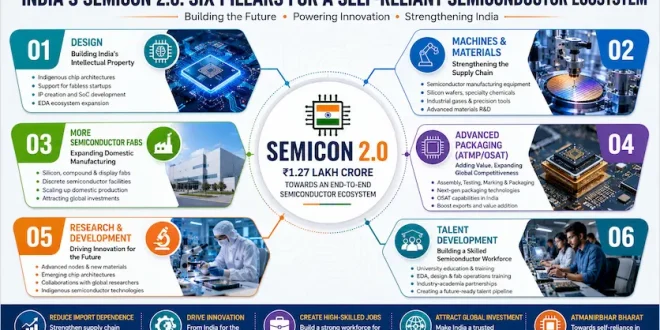
With an updated budget outlay of ₹1.27 lakh crore, the initiative moves beyond supporting individual chip factories to building an end-to-end semiconductor ecosystem. This exhaustive guide explores the six pillars of the Semicon 2.0 framework and how they combine to establish India’s physical silicon sovereignty.
The Six Pillars of India’s Semicon 2.0 Ecosystem
1. Design: Building India’s Intellectual Property (IP)
The first pillar focuses on transforming India from a chip design services hub into a creator of globally competitive semiconductor intellectual property.
-
What it includes: Development of indigenous chip architectures, support for fabless semiconductor startups, creation of reusable semiconductor IP blocks, System-on-Chip (SoC) development, and the expansion of the Electronic Design Automation (EDA) ecosystem.
-
Why it matters: India already has a large pool of semiconductor engineers working for global technology companies. Semicon 2.0 aims to ensure that more chips are designed, developed, and owned by Indian companies, strengthening technological self-reliance while creating new export opportunities.
2. Machines and Materials: Strengthening the Supply Chain
Semiconductor manufacturing depends on highly specialized equipment, chemicals, industrial gases, silicon wafers, and ultra-pure materials.
-
Focus Areas: Semiconductor manufacturing equipment, silicon wafers, specialty chemicals, industrial gases, precision manufacturing tools, and advanced materials research.
-
Why it matters: Building domestic capabilities in these critical inputs reduces dependence on imports, improves supply chain resilience, and helps India become a reliable partner in the global semiconductor ecosystem.
3. More Semiconductor Fabs
Fabrication plants, commonly known as fabs, are where semiconductor chips are manufactured on silicon wafers.
-
Semicon 2.0 supports: Silicon semiconductor fabs, compound semiconductor fabs, display fabrication units, discrete semiconductor manufacturing facilities, and the rapid expansion of domestic chip production capacity.
-
Expected Impact: The programme is designed to attract new domestic and international investments while accelerating India’s emergence as a global semiconductor manufacturing destination.
4. Advanced Packaging (ATMP/OSAT)
Once chips are manufactured, they must be assembled, tested, packaged, and prepared for commercial use.
-
Core Concepts: ATMP (Assembly, Testing, Marking, and Packaging) and OSAT (Outsourced Semiconductor Assembly and Test).
-
Objectives: Promote advanced chip packaging technologies, develop next-generation packaging capabilities, increase semiconductor exports, and build an integrated manufacturing ecosystem.
-
Importance: Advanced packaging has become one of the fastest-growing segments of the semiconductor industry, particularly with the rapid expansion of artificial intelligence, high-performance computing, and data center technologies.
5. Research & Development (R&D)
Innovation remains essential for long-term competitiveness in the semiconductor sector.
-
Priority Areas: Advanced semiconductor nodes, new semiconductor materials, emerging chip architectures, industry-academia collaboration, and indigenous semiconductor technologies.
-
Goal: Semicon 2.0 seeks to strengthen India’s research capabilities so that the country can contribute not only to manufacturing but also to future semiconductor innovations.
6. Talent Development
A successful semiconductor ecosystem requires highly skilled engineers, researchers, technicians, and manufacturing professionals.
-
Key Initiatives: University-based semiconductor education, EDA software training, chip design skill development, clean-room and fab operations training, industry-academia partnerships, and research fellowships.
-
Why it matters: By creating a strong talent pipeline, India aims to meet the workforce demands of both domestic semiconductor projects and global technology companies.
Synergizing the Ecosystem: How the Six Pillars Connect
| Pillar | Primary Objective |
| Design | Create Indian semiconductor IP and chip designs |
| Machines & Materials | Build a domestic semiconductor supply chain |
| Fabs | Expand semiconductor manufacturing capacity |
| Advanced Packaging (ATMP/OSAT) | Strengthen chip packaging and testing capabilities |
| Research & Development | Drive innovation in future semiconductor technologies |
| Talent Development | Build a globally competitive semiconductor workforce |
Frequently Asked Questions (FAQ)
What is the primary shift from Semicon 1.0 to Semicon 2.0?
Semicon 1.0 laid the groundwork by offering incentives to attract standalone silicon fabrication plants. Semicon 2.0 expands this vision horizontally and vertically, shifting the focus toward building a comprehensive, end-to-end local ecosystem that covers the entire value chain—raw materials, specialized gases, domestic intellectual property (IP) blocks, advanced packaging (ATMP/OSAT), and deep-tier academic research.
What do ATMP and OSAT stand for, and why are they vital?
ATMP stands for Assembly, Testing, Marking, and Packaging; OSAT stands for Outsourced Semiconductor Assembly and Test. They form the critical post-fabrication stage where raw silicon wafers are cut into individual dice, tested for defects, and encased in protective packaging. Because of the global AI hardware boom and high-performance computing needs, advanced packaging has become a high-margin bottleneck that India is actively capitalizing on.
How does the Machines and Materials pillar reduce external supply chain vulnerabilities?
Semiconductor production is highly susceptible to geopolitical shocks affecting raw materials. By subsidizing localized plants for specialty gases, ultra-pure chemicals, and precision tool manufacturing, India protects its multi-billion-dollar fabs from global logistics delays, creating a self-sustaining manufacturing loop.
Disclaimer
This article is published in alignment with editorial frameworks for educational and informational analysis regarding India’s industrial tech policies. All data points, budgetary allocations, and structural pillars are synthesized from public government circulars issued under the India Semiconductor Mission (ISM).
Related Coverage from Matribhumi Samachar English
-
To understand how this microchip revolution interacts with downstream deep-tech sectors, read about The Rise of Indigenous Defence Drones: How India Is Engineering Its New Era of Military Self-Reliance.
-
For details on how India is securing the core raw items required for high-tech components, see India Extends ₹7280-Crore Rare Earth Permanent Magnet (REPM) Scheme Application Deadline to July 29, 2026.
-
Discover how bilateral tech alliances are shaping future minerals supply lines in India Australia CECA 2026: Ushering a New Era in Trade, Tech, and Green Energy.