Mumbai. Friday, 19 June 2026
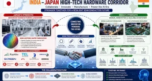
The ambition to transform India into a dominant global silicon hub has officially shifted from policy proposals directly onto the active factory floor. In a monumental boost to the India Semiconductor Mission (ISM) 2.0, Tata Electronics has signed a strategic partnership with ASML, the world’s leading supplier of advanced photolithography systems. This alliance provides the critical technological backbone for India’s first commercial front-end semiconductor fabrication plant (fab) in Dholera, Gujarat.
By integrating ASML’s advanced lithography technology with manufacturing expertise from Taiwan’s Powerchip Semiconductor Manufacturing Corporation (PSMC), the $11 billion Dholera mega-fab is positioning itself to fundamentally rewrite the global hardware supply chain.
The Four Phases of India’s High-Tech Hardware Pipeline
To move beyond basic electronics assembly and achieve true technological sovereignty, India’s semiconductor strategy segments the workflow into a precise, interconnected pipeline. Understanding where the Dholera mega-fab fits requires looking at the full spectrum of development:
-
Phase 1: Upstream Chip Design & Proprietary IP
Leveraging the government’s Design Linked Incentive (DLI) scheme, local fabless startups are breaking the old cycle of acting merely as back-offices for global tech giants. Innovations like Netrasemi’s 12nm A2000 Edge AI chip are securing native intellectual property ownership.
-
Phase 2: Front-End Fabrication (The Fab)
This is the complex chemical process of printing microscopic circuits onto raw silicon wafers. The Tata Electronics mega-fab in Dholera is built exactly for this phase, targeting a massive volume of 50,000 wafer starts per month.
-
Phase 3: ATMP & OSAT Processing (Assembly, Testing, and Packaging)
Once printed, raw wafers are sliced, packaged securely, and performance-tested. While Dholera tackles printing, active assembly operations are scaling multi-state footprints—such as Tata’s ₹27,000 crore OSAT unit in Jagiroad, Morigaon (Assam), designed to process up to 48 million chips per day.
-
Phase 4: Data Center & Industrial Integration
Finished components route directly into local AI compute clusters, automotive supply chains, and telecommunications gear.
Why Mature Nodes (28nm to 110nm) Are the Global “Sweet Spot”
A common industry misconception implies that India must print ultra-advanced 2nm or 3nm chips from day one to be successful. However, for high-volume commercial scaling and long-term economic stability, mature nodes ranging from 28nm to 110nm provide the global sweet spot.
| Industry Sector | Application Requirements | Why 28nm–110nm Node Range is Ideal |
| Automotive Electronics | Electric Vehicles (EVs), ADAS, braking systems, and power management units. | Demands extreme environmental reliability, thermal stability, and proven architectural durability rather than bleeding-edge shrinkage. |
| AI Data Infrastructure | Edge AI controllers, localized sensor arrays, and IoT hardware. | Balances high power efficiency and lower manufacturing costs for widespread edge deployment. |
| Industrial Automation | Factory robotics, process control machinery, and telemetry systems. | Provides heavily audited, reliable fabrication margins that protect operations against harsh operational conditions. |
| Telecom Gear | Routing modules, 5G base stations, and next-generation communications. | Relies on the mature nodes’ optimal balance of RF (Radio Frequency) performance and cost efficiency. |
Overcoming the “Rocky Road” of Semiconductor Infrastructure
Establishing a high-volume commercial fab requires navigating severe technical and capital barriers. Upstream manufacturing equipment installation typically consumes roughly 65% of a completely new facility’s capital layout, highlighting why the alliance with a global giant like ASML is so critical.
Beyond the machines, two fundamental grid dependencies dictate chip survival:
-
Pure Water and Power Grid Continuity: A typical commercial semiconductor fab consumes millions of gallons of water daily and demands absolute, uninterrupted clean electrical energy. A voltage fluctuation lasting even a fraction of a second can ruin an entire production batch of silicon wafers. To counter this, smart complexes are utilizing advanced predictive frameworks to stabilize manufacturing margins against minor grid ripples.
-
The Talent Ecosystem: The Tata-ASML collaboration extends far beyond heavy machinery. The two companies are co-developing semiconductor talent pipelines, advanced lithography skill-building programs, and long-term R&D frameworks. This protects the ecosystem from the “first-generation talent gap” by training domestic workforces to manage the world’s most complex machinery.
As structural investments under ISM 2.0 solidify, the symbiosis of domestic fabrication and sovereign computing networks ensures that India is no longer just planning a tech ecosystem—it is actively preparing to print its high-tech destiny.
Frequently Asked Questions (FAQ)
1. What is the difference between front-end fabrication and ATMP/OSAT processing?
Front-end fabrication (Phase 2, which is being set up in Dholera) involves the complex chemical and photolithographic process of printing micro-circuits directly onto raw silicon wafers. ATMP/OSAT (Phase 3, like Tata’s plant in Assam) takes those printed wafers, cuts them into individual dies, packages them into protective housings, and runs stress tests before final deployment.
2. Why is ASML’s involvement considered a game-changer for India?
ASML is the world’s undisputed leader in photolithography systems, which are the fundamental machines used to project circuit designs onto silicon. Securing a strategic partnership with ASML guarantees Tata Electronics access to advanced lithography solutions, equipment maintenance, and supply chain resilience initiatives critical to running a high-volume fab.
3. Will the Dholera fab make advanced 3nm chips for the latest premium smartphones?
No. The Dholera facility, in partnership with PSMC, is intentionally focusing on mature nodes ranging from 28nm to 110nm. These nodes represent the absolute commercial “sweet spot” for high-volume sectors like automotive electronics, industrial robotics, 5G modules, and Edge AI devices.
Relevant References and Deep Dives
To discover more about how active factory deployment and hardware pipelines are reshaping the nation, explore the complete investigative coverages from Matribhumi Samachar:
-
Learn how active factory deployment is flipping the script to physical infrastructure: Silicon Sovereign: How India’s Semiconductor Push is Flipping the Switch to Active Production
-
Discover the broader evolution of the high-tech hardware landscape: Silicon Sovereign: How India Semiconductor Mission 2.0 is Transforming the Global Chip Landscape
-
Read about how localized testing assets plug critical gaps in domestic IP qualification: Silicon Sovereignty: How IISc’s New Testing Lab Plugs the Critical Gap in India Semiconductor Mission 2.0
-
Analyze how structural tech investments move in tandem with massive manufacturing transformations: The Silicon and Steel Revolution: Inside India’s High-Tech Manufacturing Metamorphosis
Disclaimer
Disclaimer: The analysis and details provided in this article are based on public announcements regarding the corporate partnerships, industrial policies, and project milestones under the India Semiconductor Mission up to mid-2026. Real-world fabrication timelines, equipment installation phases, and production outputs are subject to corporate executions, supply chain dynamics, and regulatory modifications.