Mumbai. Sunday, 14 June 2026
India’s trajectory toward becoming an indispensable pillar of the worldwide high-tech supply chain has officially shifted from executive blueprints onto active factory floors. While multi-billion-dollar headlines are frequently dominated by front-end fabrication mega-projects, a critical structural correction has quietly taken place in India’s deep-tech capital.
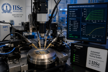
The inauguration of a state-of-the-art semiconductor testing laboratory at the Indian Institute of Science (IISc), Bengaluru, marks a pivotal milestone. Established by homegrown deep-tech startup AGNIT Semiconductors with an investment of approximately ₹3 crore, this facility provides the country with the localized validation infrastructure required to achieve complete technology sovereignty.
Why Testing and Qualification Dictate Chip Survival
Under the revised framework of the India Semiconductor Mission (ISM) 2.0, the domestic hardware pipeline is divided into four precise phases:
-
Upstream Chip Design & Proprietary IP
-
Front-End Fabrication (The Fab printing circuits on raw silicon)
-
ATMP & OSAT Processing (Assembly, Testing, Marking, and Packaging)
-
Data Center & Industrial Integration
Historically, India has been a powerhouse for Phase 1, hosting a massive microchip engineering workforce. However, the country retained virtually zero proprietary intellectual property (IP) and remained heavily dependent on international facilities for testing and qualification.
Without advanced domestic testing, an innovative design cannot be commercialized. Before any semiconductor device can power an electric vehicle, a smartphone, or a defense system, it must pass rigorous stress tests.
The Five Core Parameters Evaluated at the New IISc Lab:
-
Electrical Performance: Validating that the circuit handles exact voltage and power criteria.
-
Thermal Stability: Ensuring components can operate seamlessly without overheating.
-
Extreme Condition Reliability: Testing performance under severe environmental or operational stress.
-
Signal Integrity: Confirming data streams transmit cleanly across the architecture without distortion.
-
Long-Term Durability: Guaranteeing that the hardware won’t degrade prematurely over years of deployment.
By addressing these validation markers natively, the new IISc laboratory removes a massive logistical bottleneck, drastically slashing development timelines and capital burn for Indian deep-tech startups.
Charging the Future: A Strict Focus on Gallium Nitride (GaN) Technology
While mainstream foundries—like the upcoming Tata Electronics-PSMC facility in Dholera, Gujarat—are focusing on traditional silicon processing nodes to anchor market stability, the IISc-AGNIT facility is optimized for next-generation Gallium Nitride (GaN) technology.
GaN is rapidly outpacing traditional silicon in high-performance and high-frequency environments due to its distinct physics advantages:
| Material Characteristic | Industrial Impact & Advantage |
| Higher Power Efficiency | Drastically cuts energy loss in high-voltage operations. |
| Faster Switching Speeds | Crucial for processing massive data loads rapidly. |
| Superior Thermal Management | Chips remain cooler under load, removing bulky cooling needs. |
| Smaller Device Footprints | Allows components to shrink while delivering higher power output. |
Strategic Sectors Relying on GaN:
-
Telecommunications: Essential for the high-frequency demands of 5G and upcoming 6G network architectures.
-
Electric Mobility (EVs): Greatly improves onboard battery management networks and charging circuit efficiencies.
-
Defense & Aerospace: Powers advanced radar components, satellite payload electronics, and electronic warfare infrastructure.
Fact Check: Moving from Outlines to Real Assets
The Common Misconception: Many general overviews imply that India’s domestic semiconductor goals mean the country must print ultra-advanced 2nm or 3nm smartphone chips entirely locally from day one to be successful.
The Industrial Reality: As highlighted in extensive tech reporting across the country, building a resilient ecosystem requires a diversified approach. For high-volume commercial scaling, mature nodes (28nm to 110nm) provide the global economic “sweet spot.” Simultaneously, early-stage deep-tech startups must focus on capturing localized IP and post-silicon validation.
A prime example of this model in action is the Kerala-based fabless startup Netrasemi, which recently successfully completed the post-silicon bring-up validation for its indigenous 12nm A2000 Edge AI chip. The integration of AGNIT Semiconductors’ testing facility at IISc’s Centre for Nano Science and Engineering (CeNSE) builds a similar bridge—combining academic brilliance with industry capital to keep proprietary technology native.
Economic Convergence: Silicon Meets AI Infrastructure
The global semiconductor market is on a steady march to exceed $1 trillion in value over the next decade. As geopolitical realities make supply-chain security synonymous with national security, localized testing assets are just as vital as massive manufacturing foundries.
Furthermore, India’s chip ecosystem is scaling in absolute tandem with a regional AI compute boom. From custom liquid-cooled hyperscale data centers being built to handle generative AI workloads to specialized edge-AI controllers utilized in the automotive sector, every piece of hardware requires domestic qualification to guarantee zero supply chain friction.
By bringing advanced testing infrastructure directly into institutions like IISc, India ensures it is no longer just a back-office for global technology giants—it is actively owning the intellectual property, qualification, and execution of its digital future.
Related Coverage from Matribhumi Samachar:
-
To discover how active factory deployment and hardware pipelines are reshaping the nation, read Silicon Sovereign: How India’s Semiconductor Push is Flipping the Switch to Active Production.
-
For an in-depth analysis of the massive commercial operations driving domestic wafer manufacturing, explore the Tata Semiconductor Plant in Dholera: Turning India’s Silicon Ambitions Into Active Production.
-
Learn how localized startups are breaking the design mold with proprietary architectures in From Blueprints to Silicon: How Netrasemi’s 12nm A2000 Chip Rewrites India’s Semiconductor Future.