 Matribhumi Samachar English


Mumbai. Sunday, 12 July 2026
Silicon chip design and fabrication sub-nanometer nodes consistently dominate global headlines. However, the raw horsepower of modern processing units no longer relies solely on how tightly transistors can be carved onto a die. As traditional scaling approaches fundamental physical boundaries, the heavy lifting of performance improvements has shifted elsewhere.
Today, the true frontiers of innovation lie in advanced semiconductor materials and packaging technologies. Together, these two pillars dictate how effectively a chip manages heat, exchanges data, survives high voltages, and integrates into complex hardware ecosystems. From high-capacity AI datacenters to electric vehicle drivetrains, the choices made in materials science and multi-die architectures are redefining modern computing limits.
What Are Semiconductor Materials? Understanding the Chemical Bedrock
Semiconductor materials occupy a unique physical sweet spot: their electrical conductivity rests precisely between that of pure conductors (like copper) and insulators (like glass). By intentionally introducing impurities—a process known as doping—engineers can fine-tune this conductivity to act as rapid, precise digital switches.
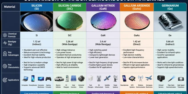
While classic silicon remains the foundation of modern technology, a new class of specialized materials has emerged to handle tasks where standard silicon falters.
1. Silicon (Si)
Silicon continues to serve as the industry workhorse, underpinning more than 90% of global semiconductor production. Thanks to decades of manufacturing maturity, it offers an incredibly cost-effective ecosystem with excellent thermal stability. It remains the default choice for mainstream computer processors, graphics units, memory chips, and standard consumer sensors.
2. Silicon Carbide (SiC)
Silicon Carbide is a wide-bandgap (WBG) semiconductor engineered specifically for harsh, high-power, and high-temperature environments. It exhibits a significantly higher voltage tolerance and lower power losses than standard silicon. This makes SiC incredibly valuable for electric vehicle (EV) powertrains, fast-charging infrastructure, solar inverters, and heavy industrial motor drives.
3. Gallium Nitride (GaN)
Another prominent wide-bandgap material, Gallium Nitride, is transforming high-frequency and power electronics. GaN features exceptionally fast switching speeds, allowing power devices to be shrunk into ultra-compact forms while emitting minimal heat. It is a critical component in 5G wireless arrays, high-efficiency commercial fast chargers, defense radar setups, and aerospace communications.
4. Gallium Arsenide (GaAs)
Known for its superior electron mobility, Gallium Arsenide delivers exceptional efficiency in high-frequency radio frequency (RF) applications. It is widely implemented inside smartphone internal transceivers, global positioning systems (GPS), and satellite communication hardware.
5. Germanium (Ge)
Though one of the earliest materials used in transistor history, Germanium has found a renewed purpose in specialized optical and high-speed devices. Its distinct physical properties make it ideal for infrared imaging sensors, fiber-optic networking lines, and specialized high-frequency transistors.
The Industrial Consumables Driving the Fab Floor
Beyond the base semiconductor substrate, fabricating an integrated circuit requires an array of ultra-pure chemical agents and supporting structural components.
-
Silicon Wafers: The foundational, ultra-flat disks sliced from single-crystal silicon ingots upon which micro-circuitry is built.
-
Photoresists: Highly light-sensitive liquid chemical polymer mixtures applied to the wafer. They react under ultraviolet light during photolithography to imprint microscale circuit patterns.
-
Photomasks: High-purity quartz plates that act as stencils, holding the exact layout designs of the chip layers used to filter light during the lithography process.
-
Specialty Gases: Highly purified gases—such as Silane, Ammonia, Argon, Nitrogen, and Hydrogen—are used to deposit chemical layers, etch away unwanted material, and handle chamber cleaning.
-
Ultra-Pure Chemicals: High-grade chemical solutions required for surface preparation, uniform wet etching, and Chemical Mechanical Planarization (CMP) to polish wafer layers smooth at an atomic level.
-
Advanced Dielectrics & Interconnects: Modern microchips employ low-resistance copper for internal wiring tracks, isolated by low-k dielectric layers (like specialized silicon dioxide variants) to stop electrical current from leaking between micro-traces.
What Is Semiconductor Packaging? Moving Beyond Simple Protection
Once the cleanroom fabrication stage concludes, the individual silicon die is incredibly fragile. Left unprotected, it would fail instantly from environmental moisture or minor physical stress.
Semiconductor packaging is the specialized engineering discipline of enclosing the silicon die in a protective housing while creating the electrical bridges needed to connect it to an external system printed circuit board (PCB). A well-designed package provides:
-
Mechanical Strength & Protection: Shielding delicate circuitry from shocks, dust, and moisture.
-
Electrical Routing: Providing the input/output (I/O) pathways for electricity and data signals to pass into the system seamlessly.
-
Thermal Dissipation: Creating a direct path for the intense heat built up by operational transistors to escape safely out of the core logic.
The Evolution Matrix of Semiconductor Packaging Technologies
Packaging has transformed dramatically from primitive through-hole pin housings into dense, multi-layered structural systems.
| Packaging Technology | Architectural Style | Distinct Advantages | Primary Use Case |
| Dual In-line Package (DIP) | Legacy Through-Hole | Simple to manufacture, durable, low-cost | Hobbyist electronics, legacy industrial hardware |
| Quad Flat Package (QFP) | Surface Mount (Peripheral) | High lead counts along four edges, thin profile | Microcontrollers, automotive control modules |
| Ball Grid Array (BGA) | Area Array (Bottom Solder) | Drastically higher pin density, superior thermal path | Mainstream PC CPUs, discrete GPUs, gaming consoles |
| Flip-Chip Packaging | Direct Die Interconnect | Eliminated wire bonds, lower latency, reduced resistance | Modern high-performance desktop processors |
| Chip Scale Package (CSP) | Ultra-Miniaturized | Package footprint closely matches the exact die size | Smartwatches, compact mobile hardware, smartphones |
| Wafer-Level Packaging (WLP) | Pre-Dicing Packaging | Massive manufacturing scale, reduced cost, ultra-thin profiles | High-density mobile transceivers, integrated sensors |
| Fan-Out WLP (FOWLP) | Next-Gen Wafer-Level | Ultra-dense I/O routing outside the physical die perimeter | Elite smartphone application processors, AI nodes |
| 2.5D Packaging | Multi-Die Substrate | Side-by-side placement on a silicon interposer, high bandwidth | Advanced AI accelerators, datacenter compute clusters |
| 3D IC Packaging | Vertical Die Stacking | True vertical stacking via TSVs, immense memory bandwidth | High-Bandwidth Memory (HBM), advanced server chips |
Advanced Thermal Management and Emerging Package Trends
As multi-die systems like chiplets and stacked 3D IC architectures become standard, heat density has risen exponentially. Stacking high-power logic dies directly adjacent to or underneath High-Bandwidth Memory (HBM) creates high-temperature hotspots that can trigger thermal throttling.
To combat this, the industry is transitioning away from basic thermal greases toward Thermal Interface Materials (TIM) with high thermal conductivity, embedded vapor chambers, and direct-die liquid cooling. In massive AI clusters, data centers are actively implementing immersion cooling, completely submerging server racks in specialized dielectric fluids to dissipate heat evenly.
Furthermore, emerging structural shifts—like replacing organic package substrates with rigid, ultra-smooth glass substrates—are allowing for even tighter interconnect densities and better dimensional stability. Similarly, hybrid bonding techniques are eliminating solder bumps entirely, allowing copper-to-copper direct connections at the atomic level for unprecedented interconnect speeds.
Global Supply Chains and Local Industrial Milestones
The escalating global demand for advanced computing hardware has shifted the semiconductor supply chain into a topic of absolute geopolitical importance. Because advanced packaging capacity remains a major global bottleneck, nations are moving quickly to secure domestic processing and materials infrastructure.
For instance, structural efforts to secure midstream material processing are expanding worldwide. A prime example is the recent extension of the Indian government’s ₹7,280-Crore Rare Earth Permanent Magnet (REPM) Manufacturing Scheme, which highlights the international push to lock down rare earth supplies critical for high-tech industrial motors, wafer-handling automation, and EV drivetrains. Simultaneously, international infrastructure pushes—such as the landmark Tata Electronics and ASML strategic partnership anchoring commercial fab facilities in Dholera—demonstrate how rapid technology transfers are distributing manufacturing nodes beyond traditional borders.
These massive fabrication developments are further accelerated by comprehensive trade alliances, like the India-Australia CECA cross-border trade framework, focusing heavily on securing steady upstream critical mineral and rare earth element access. To sustain the heavy financial burdens of deep-tech research and fabrication scaling, modern tech ecosystems are relying heavily on dedicated public-private investment pipelines, such as the Startup India Fund of Funds 2.0 initiatives providing specialized capital for deep-tech, AI, and domestic semiconductor research teams.
Frequently Asked Questions (FAQ)
Q1: Why are wide-bandgap materials like SiC and GaN preferred over traditional Silicon for power electronics?
A1: Wide-bandgap materials feature an atomic structure that requires higher energy to switch electrons from an insulating state to a conducting state. This quality enables them to withstand significantly higher voltages, operate at much higher temperatures, and switch on and off faster than standard silicon, dramatically cutting down power loss and device size.
Q2: What is the main structural difference between 2.5D and 3D semiconductor packaging?
A2: In 2.5D packaging, multiple dies (like a CPU logic die and an HBM stack) are laid out side-by-side on top of a shared silicon interposer, which routes high-speed signals horizontally between them. In 3D packaging, the dies are stacked directly on top of one another vertically, utilizing vertical Through-Silicon Vias (TSVs) to pass signals directly through the silicon layers.
Q3: How does advanced semiconductor packaging resolve the “memory wall” in AI accelerators?
A3: The “memory wall” refers to the performance bottleneck where a fast processor wastes energy and time waiting for data to arrive from far-away system memory chips. By utilizing advanced 3D packaging to stack High-Bandwidth Memory (HBM) inches or millimeters away from the main logic processor, data paths are drastically shortened, unlocking wider buses and faster processing speeds.
Q4: What role do specialty gases play inside the semiconductor fabrication plant?
A4: Specialty process gases are highly pure chemical inputs used to build up or carve out individual features on a silicon wafer. For instance, silane is frequently used to deposit silicon layers, while other reactive gases clean the chambers or etch away excess materials to leave clean circuit pathways behind.
Disclaimer: This article is provided solely for informational and educational purposes. The semiconductor manufacturing sector involves rapidly shifting technologies, corporate alliances, and policy frameworks. Readers are advised to cross-reference technical specifications and market updates with original equipment manufacturers and formal corporate releases.