 Matribhumi Samachar English


Mumbai. Sunday, 12 July 2026
The landscape of Indian electronics is undergoing a foundational paradigm shift. For decades, India has functioned as an intellectual powerhouse for the global tech ecosystem, housing thousands of engineers who design highly sophisticated processor architectures, integrated circuits, and artificial intelligence accelerators. Yet, the physical creation of these chips followed a fragmented international route: designed in Bengaluru or Hyderabad, fabricated in Taiwan, packaged in Malaysia or China, and finally shipped back for assembly into finished products.
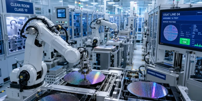
The commencement of commercial production at the Sanand OSAT (Outsourced Semiconductor Assembly and Test) facility in Gujarat alters this dynamic completely. By keeping critical midstream assembly, testing, and advanced packaging within the country, India is steadily turning its theoretical chip design dominance into a fully integrated, self-reliant semiconductor ecosystem.
What is an OSAT Facility and Why Does It Matter?
Before a semiconductor can power a device, raw silicon wafers processed at multi-billion-dollar fabrication units must undergo highly specialized transformations. This is the exact domain of the Sanand OSAT facility. It bridges the gap between raw wafer fabrication and physical device integration through five critical pillars:
-
Chip Assembly: Precision slicing of delicate silicon dies from wafers and mounting them onto protective substrates.
-
Advanced Packaging: Integrating multiple dies into high-density modules to enhance processing speeds and thermal efficiency.
-
Rigorous Testing: Subjecting every chip to simulated environments to verify performance.
-
Reliability Validation: Ensuring components can survive continuous loads across industrial lifespans.
-
Quality Assurance: Filtering out nano-scale manufacturing defects before shipping.
By executing these phases domestically, India eliminates reliance on overseas packaging corridors, shortens logistics times, and eliminates supply chain vulnerabilities. This operational baseline pairs naturally with broader macro infrastructure movements, such as the historic Tata Semiconductor Plant in Dholera, which anchors front-end manufacturing, alongside strategic supply agreements like the Tata Electronics and ASML Partnership to secure elite lithography equipment.
Powering High-Growth Deep Tech Verticals
The domestic activation of the Sanand OSAT facility directly acts as a catalyst for several highly demanding technology sectors.
1. Artificial Intelligence Infrastructure
Modern AI workloads rely heavily on advanced heterogeneous packaging—fusing specialized logic units alongside high-bandwidth memory. Having an operational OSAT presence ensures local availability of packaged components, allowing edge computing systems and localized AI servers to scale without import bottlenecks.
2. Robotics & Industrial Automation
Robotics requires deep integration of motion controllers, custom transceiver units, and vision processors. Localizing the packaging stage allows automation systems to be iteratively tested and deployed much faster. However, as noted in analyses regarding the Indigenous Defence Drones Sector, achieving absolute autonomy in these fields requires simultaneously resolving secondary choke points—such as local access to microcontrollers and high-performance sensor modules.
3. Electric Vehicles (EVs) & Green Energy
Automotive power electronics demand high thermal resilience and severe reliability validation. The expansion of domestic chip packaging fits directly into the wider strategy to secure the raw components required for modern high-torque EV motors, which is further supplemented by bilateral supply deals like the India Australia CECA Agreement for critical battery inputs like lithium and cobalt.
The Road Ahead: Overcoming Remaining Vulnerabilities
While the operationalization of Sanand marks a landmark milestone for the India Semiconductor Mission, transforming the nation into a globally competitive semiconductor center requires sustaining investments across adjacent industrial layers:
| Critical Ecosystem Needs | Strategic Focus Area |
| Upstream Substrates | Domestic processing of raw silicon wafers, specialized chemicals, and ultra-pure gases. |
| Material Supply Chains | Localizing processing loops for vital materials, exemplified by initiatives like the Rare Earth Permanent Magnet (REPM) Scheme, which powers the precision automation motors used within semiconductor clean rooms. |
| Workforce Development | Bridging engineering talent into hyper-specialized physical assembly, clean-room management, and hardware packaging domains. |
By successfully tying front-end chip design talent with operational midstream packaging hubs like Sanand and massive front-end mega-fabs, India is systematically erecting a resilient, self-sustaining electronic hardware infrastructure engineered for the decades ahead.
Frequently Asked Questions (FAQ)
What is the specific role of the Sanand OSAT facility?
The Sanand OSAT facility takes manufactured silicon wafers and processes them through assembly, testing, and advanced packaging. This turns delicate, raw silicon dies into durable, market-ready microchips optimized for smartphones, cars, and industrial servers.
Why is an OSAT plant vital if India already excels at chip design?
Design is only the blueprint stage. Historically, chips designed in India had to be sent overseas to countries like Malaysia or China for physical assembly and testing. Domestic OSAT facilities bring that vital middle step onshore, reducing transport costs, improving security, and speeding up production timelines.
How does the Sanand facility support India’s AI and robotics ambitions?
Advanced AI and robotics hardware require high-density multi-chip modules that bundle processing speed with precise energy management. Local OSAT infrastructure ensures that custom AI accelerators and robotics controllers can be reliably packaged, validated, and scaled inside domestic assembly corridors.
Disclaimer
This article is for informational and educational purposes only. The information regarding industrial projects, timelines, policy subsidies, and supply chain developments is based on public disclosures available at the time of publication. Readers should independently verify technical metrics or investment allocations before making financial or business decisions.