

Mumbai. Friday, 17 July 2026
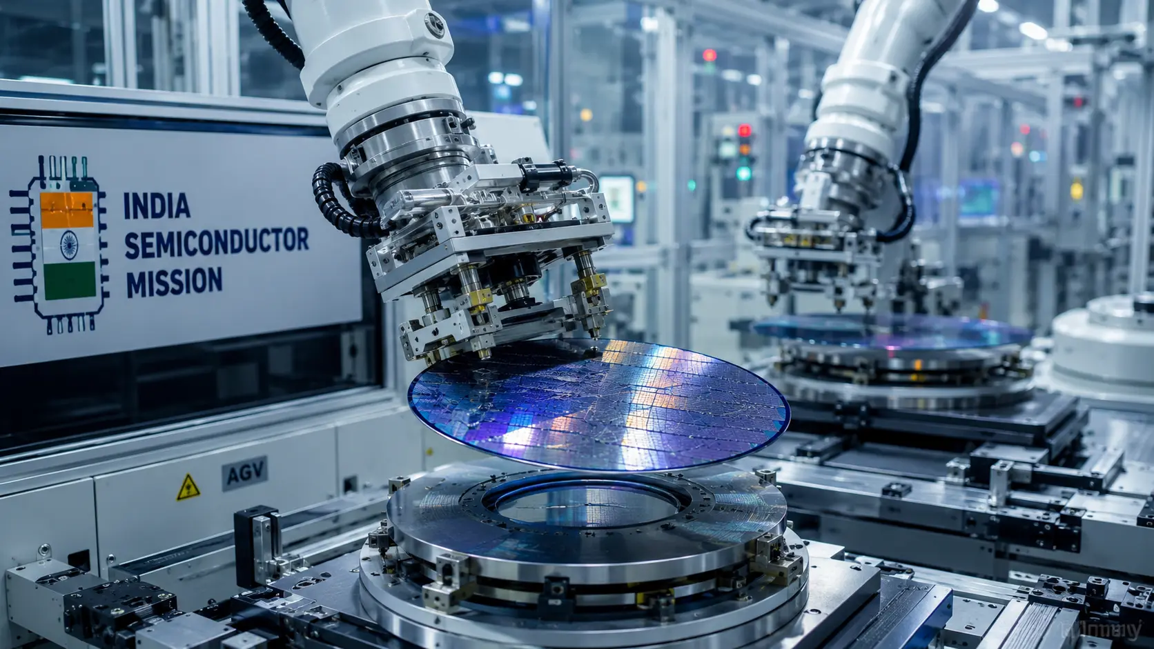
India’s transition from a software outsourcing destination into a physical, deep-tech manufacturing superpower has officially crossed a critical threshold. Under the structured backing of the India Semiconductor Mission (ISM) and the newly active Semicon 2.0 programme, the nation’s chip ambitions are no longer mere legislative goals. They have materialized into a massive ₹2.87 lakh crore sovereign architectural pivot, creating an end-to-end electronics layout spanning six key industrial states.
By scaling up infrastructure, building direct synergy with adjacent electronics schemes, and expanding upstream supply chains, India is rewriting its role in the global technology supercycle.
The Strategic Catalyst: Why India Is Racing for Silicon
Semiconductors serve as the fundamental nervous system for modern technology—powering everything from everyday consumer electronics to Electric Vehicles (EVs), AI data centers, and defense platforms. With the Union Cabinet actively passing sweeping capital injections—such as the massive ₹62,500 crore Mobile Phone Manufacturing Scheme (MPMS)—domestic chip production has shifted from a financial luxury to a strict geopolitical necessity.
To completely insulate its hyper-growing local industries from global supply shocks, the Indian government committed a historic ₹1.6 lakh crore under the initial phase of the semiconductor mission. In 2026, the introduction of Semicon 2.0 adds a fresh ₹1.27 lakh crore package, specifically designed to accelerate upstream material capacities, design startups, and localized commercial production.
The Six Pillars: Mapping the Nationwide Semiconductor Ecosystem
Rather than concentrating production in a single geographic pocket, India has deployed a diversified, multi-state factory cluster model. Each region leverages its specific logistical, geographical, or structural strengths:
1. Gujarat – The Epicenter of Commercial Production
Gujarat stands as the structural anchor of India’s hardware dreams. The state’s well-integrated port infrastructure and robust power grids have converted the region into an active manufacturing zone.
Micron Technology (Sanand): The marquee $2.75 billion Assembly, Testing, Marking, and Packaging (ATMP) plant successfully transitioned into full-scale commercial operations in early 2026, feeding processed memory modules into global supply networks.
CG Semi & Kaynes Semicon: Operating inside the high-tech electronics parks, these Outsourced Semiconductor Assembly and Test (OSAT) facilities are actively delivering packaged microchips tailored for automotive systems, smart mobility, and industrial industrial units.
Tata Electronics & PSMC (Dholera): Construction is advancing aggressively on India’s premier multi-billion-dollar silicon fabrication plant, laying the physical groundwork for legacy node commercial manufacturing.
2. Assam – The Northeast’s High-Tech Breakthrough
Breaking the historical mold of industrial distribution, Assam has entered the deep-tech map via Tata Electronics’ massive ₹27,000 crore semiconductor assembly and advanced packaging facility in Jagiroad. This deployment is engineered to anchor an entirely new downstream industrial supply line across Northeast India, introducing thousands of precision engineering jobs to the region.
3. Uttar Pradesh – The Display and Compute Capital
Complementing the thriving consumer electronics hubs across Noida and Greater Noida, Uttar Pradesh has successfully secured specialized display fabrication projects. Led by major cross-border initiatives, including the high-profile HCL-Foxconn project at Jewar, the state is harmonizing raw semiconductor packaging with advanced display panel integration.
4. Andhra Pradesh – The Advanced Logistics and Packaging Gateway
Andhra Pradesh is capitalizing on its strategic deep-water coastline and dedicated electronic manufacturing clusters (EMCs). The state is absorbing substantial investment inflows focused on high-density semiconductor packaging and component logistics, bridging the gap between local production and international shipping corridors.
5. Odisha – The Core Mineral and Heavy Industrial Base
Odisha is converting its vast heavy-industrial infrastructure and mineral wealth into an advanced manufacturing springboard. By coupling semiconductor component processing with the country’s broader clean energy and materials initiatives, Odisha is carving out a niche in handling the foundational resources required for raw technology development.
6. Rajasthan – The Component Frontier
Rajasthan has officially debuted on the microchip map through Sahasra Semiconductors’ specialized ATMP/OSAT installation in Bhiwadi. Situated perfectly inside a rapidly growing Electronics Manufacturing Cluster, the facility is successfully rolling out localized semiconductor memory cards and foundational component packaging.
The Semicon 2.0 Evolution: Engineering the Closed-Loop Supply Chain
What truly sets the 2026 semiconductor push apart is the strategic understanding that a factory cannot survive without a secure ecosystem. To prevent local fabs from remaining dependent on imported materials, Semicon 2.0 extends capital incentives deeply into the midstream and upstream supply chains:
Upstream Synergy: The policy explicitly integrates alongside allied initiatives like the ₹7,280-crore Rare Earth Permanent Magnet (REPM) Scheme, ensuring that precision components used in clean-room automated wafer handlers and robotics are manufactured domestically.
Design Sovereignty: Rather than just assembling foreign intellectual property, the India Semiconductor Mission has empowered over 105 indigenous chip design startups. This focus on domestic architectural creation is yielding vital milestones, allowing local companies to leverage open-source architectures like RISC-V for domestic telecommunications and defense networks.
Comprehensive Resource Mapping: Fresh incentives are successfully drawing international partnerships from technological leaders like Japan and South Korea, drawing specialized chemical houses, industrial gas refiners, and extreme-purity water treatment corporations right onto Indian soil.
Moving from Policy to Real-World Output
With multiple packaging lines currently churning out commercial products and massive silicon fabs systematically moving toward their next phases of commissioning, India is actively shedding its historical reliance on imported silicon foundries. By building an interconnected web across six distinct states, the nation is successfully safeguarding its industrial sovereignty—securing a resilient seat at the high-stakes table of the global semiconductor supply chain.
Frequently Asked Questions (FAQ)
Q1: What is the main difference between Semicon 1.0 and Semicon 2.0?
Semicon 1.0 focused primarily on establishing the absolute basics—approving primary mega-fabs and massive packaging facilities. Semicon 2.0 expands the total financial layout to ₹1.27 lakh crore, moving heavily into the upstream ecosystem by subsidizing raw chemicals, specialty gases, equipment manufacturing, and long-term research and development.
Q2: What do ATMP and OSAT mean in chip manufacturing?
ATMP stands for Assembly, Testing, Marking, and Packaging, while OSAT stands for Outsourced Semiconductor Assembly and Test. These facilities do not carve the microscopic circuits onto raw silicon; instead, they take finished silicon wafers, cut them into individual dice, test them for errors, and package them into the protective protective shells that can be soldered onto circuit boards.
Q3: Which facilities are already running commercial production in India?
As of early 2026, Micron Technology’s massive facility in Sanand, alongside dedicated packaging units from CG Semi and Kaynes Semicon in Gujarat, have fully crossed the threshold from pilot trials into active, large-scale commercial output.
Q4: How does domestic chip production help India’s defense and EV sectors?
Currently, critical systems like automotive Electronic Control Units (ECUs) and defense equipment (such as UAV guidance units) rely heavily on international silicon foundries. Localizing the packaging and manufacturing pipelines ensures total data security, protects equipment from foreign backdoor vulnerabilities, and eliminates supply bottlenecks.
Disclaimer: This article is prepared strictly for informational, educational, and journalistic purposes. The economic metrics, investment figures, and project timelines are compiled from recent ministerial announcements, policy declarations, and industrial data available under the India Semiconductor Mission guidelines as of July 2026.
Related Deep-Tech Insights from Matribhumi Samachar English:
To explore the complete architectural framework of the newly expanded semiconductor roadmap, read the full analysis on the India Semiconductor Mission 2.0: The Rise of India’s High-Tech Microchip Manufacturing Ecosystem.
To understand how regional industrial clusters are transforming northern India, see the breakdown on Silicon Sovereign: How Uttar Pradesh is Powering Up as India’s Next High-Tech Manufacturing Hub.
Discover how critical mineral access is securing the raw inputs for domestic wafer manufacturing via the India Australia CECA 2026: Ushering a New Era in Trade, Tech, and Green Energy.
Learn about the vital magnet and equipment components driving clean-room robotics in the official update on the India Extends ₹7280-Crore Rare Earth Permanent Magnet (REPM) Scheme Application Deadline to July 29, 2026.
