 Matribhumi Samachar English


Mumbai. Saturday, 18 July 2026
India’s industrial architecture is undergoing a monumental paradigm shift. Moving aggressively beyond its historic reputation as a software outsourcing hub, the country has crossed a critical threshold into deep-tech, physical manufacturing. Backed by the Union Cabinet and structured under the India Semiconductor Mission (ISM), the newly active Semicon 2.0 program signals a deliberate pivot from approving isolated production units to anchoring an all-inclusive, self-reliant semiconductor ecosystem.
With an expanded fiscal roadmap, this second phase aims to incentivize every node of the value chain—spanning front-end fabrication, back-end packaging, raw materials supply, tool access, and world-class workforce development.
The Massive Fiscal Expansion of Semicon 2.0
To fully comprehend the scale of Semicon 2.0, one must look at the capital infusion. Building upon the foundational framework of early Production Linked Incentive (PLI) strategies, India has expanded its strategic semiconductor deployment to an impressive financial outlay. The revamped policy architecture targets deep vertical integration with an overarching objective of driving trillions of rupees in total industrial investments by the end of the decade. The mission’s primary target is enabling India to own core chip intellectual property (IP) and globally competitive design patents rather than just operating as a generic contract assembly floor.
Phase 1 (2026): The Foundation & Incentive Rollout
The year 2026 serves as the primary deployment vector for expanding paracapital distribution across the entire semiconductor value chain. Rather than treating sections of the lifecycle as disjointed sectors, the updated policy provides targeted subsidies across eight critical divisions:
-
Silicon Fabrication (CMOS Fabs): Large-scale commercial foundries handling standard nodes receive a 40% Capex subsidy distributed on a pari-passu (equal footing) basis.
-
Specialty Fabs: Dedicated facilities focused on compound semiconductors, discrete components, and display driver units qualify for a 35% Capex subsidy.
-
Back-End Facilities (ATMP & OSAT): Advanced packaging setups (3D packaging and heterogeneous integration) receive a 35% Capex subsidy, while conventional legacy packaging units get 25%.
-
Upstream Materials & Machinery: Introducing financial offsets to de-risk localized production of specialty chemicals, high-purity industrial gases, and advanced semiconductor testing equipment.
-
Fabless Design Ecosystem: The expanded Design Linked Incentive (DLI) scheme now allows large domestic private conglomerates—alongside startups and MSMEs—to access risk capital, subsidized Electronic Design Automation (EDA) tools, and direct tape-out fund matching.
Phase 2 (2027): Manufacturing Begins to Scale
By 2027, the emphasis transitions from policy underwriting to active, scaled operations. Early manufacturing wins funded during the early stages of the semiconductor mission will cross the threshold from factory construction into commercial pilot runs.
Target Verticals for Early Silicon Yields:
-
Automotive Chips: Feeding the massive global electric vehicle (EV) and smart mobility supply chains.
-
Power Management Integrated Circuits (PMICs): Serving power-grid components and device power delivery.
-
Display Drivers & Industrial Electronics: Powering automated machinery and domestic hardware arrays.
This phase deliberately converges with parallel manufacturing schemes, such as the Mobile Phone Manufacturing Scheme (MPMS). By offering added sales incentives to consumer device brands that source locally packaged microchips, the government has engineered an internal demand loop. Simultaneously, major logistics pipelines will focus on localized supply chain materials—including photoresists, packaging substrates, and chemical mechanical planarization (CMP) elements—to insulated facilities from global import disruptions.
Phase 3 (2028): Ecosystem Matures into a Global Hub
The year 2028 is mapped out as the milestone horizon where India’s first commercial silicon fabrication mega-fabs are projected to stabilize production. Concurrently, a multi-state network of operational ATMP and OSAT facilities will enter full commercial capacity.
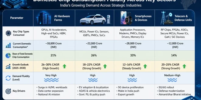
┌────────────────────────────────────────────────────────┐
│             DOMESTIC CHIP CONSUMPTION FLUIDITY         │
├───────────────────────────┬────────────────────────────┤
│    AI Hardware Farms      │ Automotive Systems & EVs   │
├───────────────────────────┼────────────────────────────┤
│ Smartphones & Devices     │ Telecom & Defense Units    │
└───────────────────────────┴────────────────────────────┘
The resulting high-yield environment positions the country to compete openly with established global semiconductor hubs, transforming it from a pure importer of complex processors into an international exporter of advanced packaged silicon.
The Human Capital Engine: Workforce Development Roadmap
Hardware cannot function without human expertise. The state is institutionalizing a standardized high-tech training curriculum rolled out across more than 320 universities nationwide. Utilizing shared EDA platforms, the goal is scaling the specialized workforce past the initial pool of 70,000 engineers. The learning roadmap shifts away from theoretical design toward critical operational skill sets:
-
VLSI & Physical Design Verification
-
Cleanroom Operations & Yield Engineering
-
Process Engineering & Equipment Maintenance
-
Advanced Packaging & Reliability Testing
Structural Timeline: Milestones at a Glance
| Year | Expected Core Milestone | Focus Vectors |
| 2026 | Multi-tiered incentive rollout, expanded DLI program activation, project sanctions. | Silicon Fabs, OSAT/ATMP, Specialty Materials, Fabless Startups. |
| 2027 | Initial back-end production begins, pilot wafer runs, upstream supply localization. | PMICs, Automotive Microcontrollers, Localized Gases/Photoresists. |
| 2028 | Commercial mega-fabs commissioned, export-ready volume expansion, global ecosystem maturity. | AI Processors, Advanced 3D Packaging, Mass Silicon Wafers. |
Critical Challenges on the Horizon
Despite unmatched momentum, the road ahead requires addressing structural friction points:
-
Infrastructure Lead Times: Ensuring continuous, zero-fluctuation power grids and ultra-pure water pipelines during fab commissioning.
-
Global Supply Interdependencies: Procuring and maintaining proprietary lithography machines and extreme ultraviolet (EUV) tools amid competitive geopolitical global demand.
-
Certification Bottlenecks: Managing the long qualification and validation cycles mandatory for aerospace, automotive, and defense electronics before mass production begins.
Outlook: A Sovereign Tech Future
Semicon 2.0 represents a clear evolution in industrial planning. By shifting from the isolated project approvals of Phase 1 to a unified, multi-tiered infrastructure network, India is laying the foundations for decades of deep-tech self-reliance. If this momentum maintains its current heading through 2028, it will decisively establish India as an indispensable pillar of the global high-tech microchip supply chain.
Frequently Asked Questions (FAQ)
Q1: What makes Semicon 2.0 different from the first phase of the India Semiconductor Mission?
A: Phase 1 focused primarily on attracting individual mega-fab applications. Semicon 2.0 shifts the focus toward building the entire ecosystem by heavily subsidizing the upstream raw materials, specialty gases, design houses, and back-end assembly facilities required to sustain a fab locally.
Q2: What are the exact Capex subsidy rates offered under Semicon 2.0?
A: The policy offers a 40% Capex subsidy on a pari-passu basis for CMOS Silicon Fabs, a 35% Capex subsidy for Specialty and Compound Fabs, a 35% subsidy for Advanced Packaging (ATMP/OSAT), and a 25% subsidy for legacy packaging facilities.
Q3: Which industries will benefit the most from this mission?
A: Downstream sectors like electronics manufacturing services (EMS), automotive companies, AI hardware firms, telecommunications equipment developers, and defense electronics will benefit from direct access to domestically produced, secure silicon components.
Disclaimer:
The analytical conclusions, projections, and policy breakdowns outlined in this article are for informational and educational purposes based on current 2026 industrial frameworks. Actual manufacturing timelines, asset disbursements, and corporate commissioning dates remain subject to individual corporate execution schedules, global component availability, and regulatory modifications.
External References
-
For the latest real-time business context and industrial rollouts across India, read updates on Matribhumi Samachar English Main Portal.
-
Learn about parallel technology milestones by visiting the India Semiconductor Mission 2.0 Deep Dive on Matribhumi Samachar.
-
To discover how early facilities have transitioned into functional output, see the comprehensive report on Silicon Sovereign: How India’s Semiconductor Push is Flipping the Switch to Active Production.