

Mumbai. Monday, 20 July 2026
India’s ambition to establish itself as a globally recognized chip powerhouse has reached a critical turning point. Moving decisively beyond its historical strengths in IC (integrated circuit) design, software automation, and back-end assembly, the nation is steadily forging a presence in the most complex, capital-intensive segment of the microelectronics ecosystem: semiconductor manufacturing equipment engineering.
At the center of this transformation is Applied Materials India, whose expanding operations in Bengaluru highlight how the country is evolving from a software talent destination into a strategic hub for hardware prototyping, equipment qualification, and process engineering.
Bengaluru: The Strategic Hub for High-Precision Engineering
As global semiconductor demand accelerates, the equipment required to execute sub-nanometer atomic layer deposition, chemical mechanical planarization (CMP), and plasma etching has become a central focus of technological independence. Applied Materials has scaled its Bengaluru operations into one of its largest research and development centers outside the United States.
Rather than serving purely as an offshore support office, engineering teams in Bengaluru operate across full-lifecycle product development disciplines:
System & Mechanical Architecture: Designing high-precision vacuum chambers, thermal distribution systems, and robotic wafer transfer handlers.
Process Engineering & Simulation: Modeling plasma dynamics, chemical reaction flows, and atomic-scale material behaviors.
Control Systems & Automation Software: Developing real-time embedded systems that manage wafer transport and equipment safety.
Reliability & Validation Engineering: Conducting stress testing, component failure analysis, and operational validation.
The India Validation Center (IVC): Local Prototyping on 300 mm Wafers
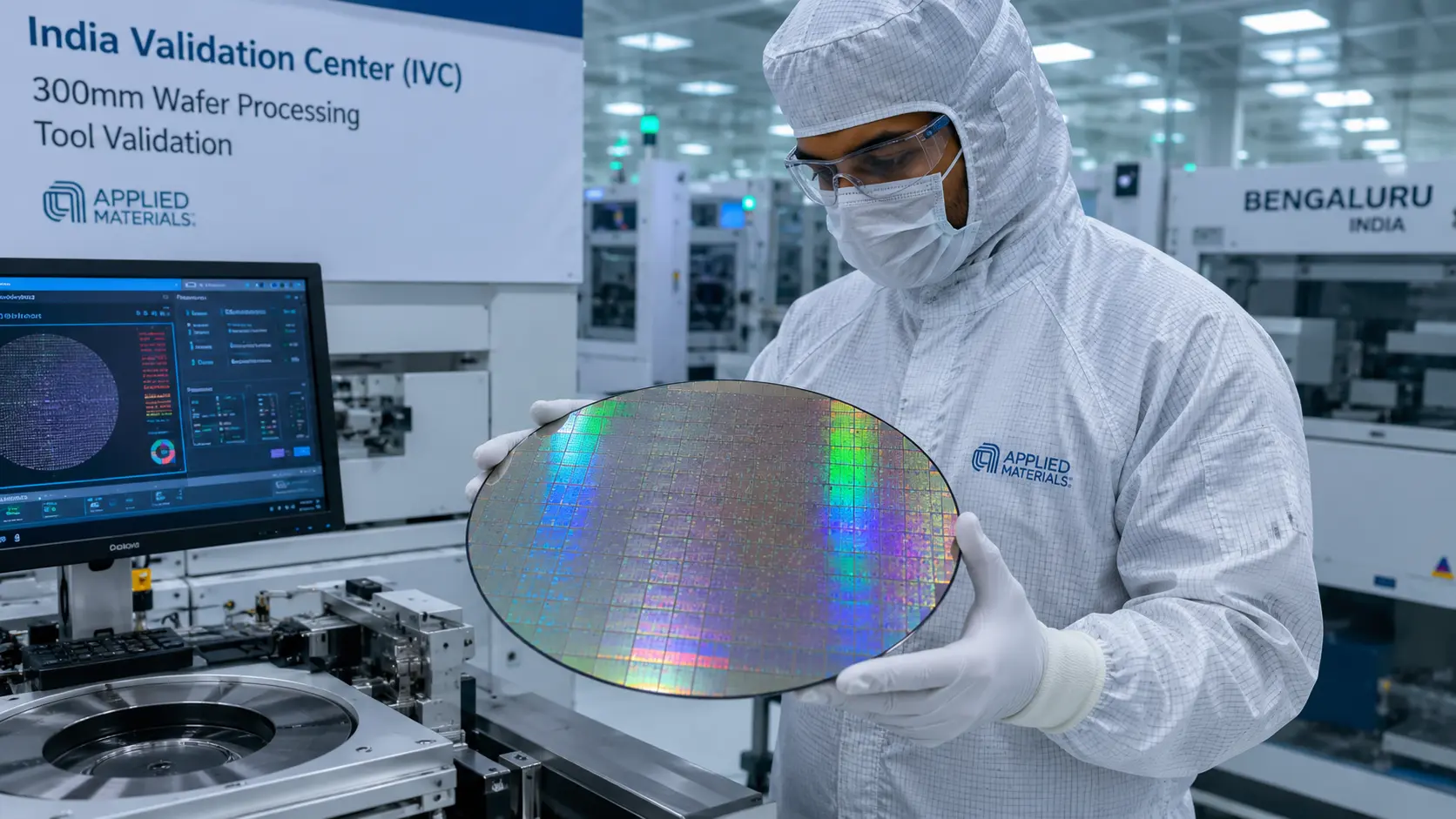
A key driver of this regional evolution is the operational rollout of the India Validation Center (IVC) in Bengaluru.
Historically, domestic engineering concepts or modifications had to be sent to overseas fabrication facilities in North America or East Asia for physical validation. The IVC changes this dynamic by offering localized access to industry-standard 300 mm silicon wafers operating within state-of-the-art cleanroom environments.
[Design & Simulation] ➔ [Local Prototyping] ➔ [300 mm Wafer Testing at IVC] ➔ [Global Fab Deployment]
The facility directly supports:
Equipment Qualification: Ensuring tools meet micro-scale process tolerances.
Process Optimization: Fine-tuning physical gas flows, temperatures, and deposition rates.
Prototype Evaluation: Iterating on hardware builds in real time without international shipping delays.
Reliability & Yield Verification: Testing tool durability under simulated continuous-production fab environments.
From Engineering Support to Full Product Ownership
This infrastructure enables Applied Materials India to expand its scope beyond tactical tasks into core product ownership. Indian engineers are increasingly leading initiatives across:
Next-Generation Platforms: Architecting underlying tool platforms for advanced node logic and memory fabrication.
IP Generation: Filing patents globally for novel mechanical designs, automated diagnostic routines, and material handling solutions.
Integrated Artificial Intelligence: Embedding predictive analytics directly into tool control software to forecast component wear, minimize unscheduled fab downtime, and improve wafer yield.
Strengthening the Domestic Ecosystem & Supply Chain
The expansion of upstream equipment engineering aligns with the goals of the India Semiconductor Mission (ISM) and the Semicon 2.0 framework. As commercial fabs—such as Tata Electronics’ 300 mm facility in Dholera—come online, having an equipment engineering ecosystem nearby offers distinct regional advantages:
Deep-Tech Talent Cultivation: Training specialized mechanical, mechatronic, and materials engineers adept at handling atomic-scale manufacturing requirements.
Precision Supplier Growth: Encouraging domestic machine shops, specialty metal fabricators, and cleanroom vendors to achieve the precision tolerances required for global fab equipment.
Academic Research Collaboration: Partnering with premier institutes (such as IISc and top IITs) to bridge fundamental materials science research with commercial equipment manufacturing.
Why Upstream Equipment Matters
Building semiconductor fabs requires significant capital, but mastering the equipment that builds the chips establishes long-term technological capability. Equipment vendors occupy an irreplaceable position in the global supply chain, serving as the link between materials science theory and practical manufacturing.
Applied Materials India’s trajectory demonstrates that India’s tech ecosystem is taking on higher-value responsibilities. By combining software capabilities, artificial intelligence integration, and high-precision physical engineering, the country is anchoring its role as an essential partner in global semiconductor manufacturing.
Visual Context: Advanced Wafer Handling Equipment
Frequently Asked Questions (FAQ)
Q1: Why is 300 mm wafer capability at the India Validation Center significant?
A: 300 mm silicon wafers are the global standard for high-volume, advanced node microchip production. Local 300 mm testing allows engineers in India to validate physical tools and processes under exact commercial fab conditions without relying on overseas facilities.
Q2: How does equipment engineering differ from chip design?
A: Chip design focuses on architecting micro-scale logic circuits on software layout platforms. Equipment engineering builds the physical machinery—including vacuum systems, plasma etch chambers, robotics, and fluid dynamic tools—used to physically print those designs onto silicon.
Q3: How does this development support the India Semiconductor Mission (ISM)?
A: While ISM subsidies encourage fab construction, equipment engineering builds local technical knowledge, precision manufacturing capabilities, and an IP foundation necessary for a sustainable semiconductor supply chain.
Disclaimer
This article is intended for informational and educational purposes. Corporate brand names, trademarks, and initiatives referenced (including Applied Materials and the India Semiconductor Mission) belong to their respective owners. Views expressed reflect industry developments in semiconductor engineering and policy as of 2026.
Relevant Coverage & Further Reading
For further analysis on India’s deep-tech manufacturing transformation, electronics policy, and supply chain shifts, explore the following editorial reports:
