

Mumbai. Sunday, 19 July 2026
India’s bold transition from a global chip design powerhouse into a comprehensive physical manufacturing giant has officially crossed into its next critical phase under the structured backing of the India Semiconductor Mission (ISM) and the newly active Semicon 2.0 framework.
While capital subsidies and multi-billion-dollar investments have successfully catalyzed the construction of front-end fabrication plants (Fabs) and advanced packaging (ATMP/OSAT) hubs across the nation, an underlying strategic truth remains: building a chip requires control over a hyper-specialized upstream supply chain. A modern semiconductor ecosystem depends on hundreds of advanced chemicals, high-purity gases, ultra-flat substrates, and rare elements. To build resilient, long-term sovereignty, India must bridge the heavy reliance on imported midstream and upstream materials.
1. Silicon Wafers: Crossing the Foundational Hurdle
Every integrated circuit begins its life on an ultra-pure slice of electronic-grade silicon. Despite India holding massive raw quartz reserves, the complex technological steps required to transform raw silicon dioxide into commercial wafers remain highly concentrated in foreign markets like Japan, Taiwan, and Germany.
To eliminate this bottleneck, local industrial groups are actively evaluating technology transfers to scale localized production across four core pillars:
Electronic-Grade Polysilicon: Refining raw silicon to a mandatory 99.999999999% (11N) purity level.
Monocrystalline Ingot Pulling: Cultivating massive single-crystal structures with zero lattice defects.
200mm & 300mm Wafers: Scaling up high-precision diamond slicing and polishing lines to feed emerging commercial fabs.
Epitaxial Growth: Depositing engineered crystalline layers directly onto raw wafers to establish specialized electrical baselines.
2. Specialty Chemicals & Photoresists: The Ultra-Purity Challenge
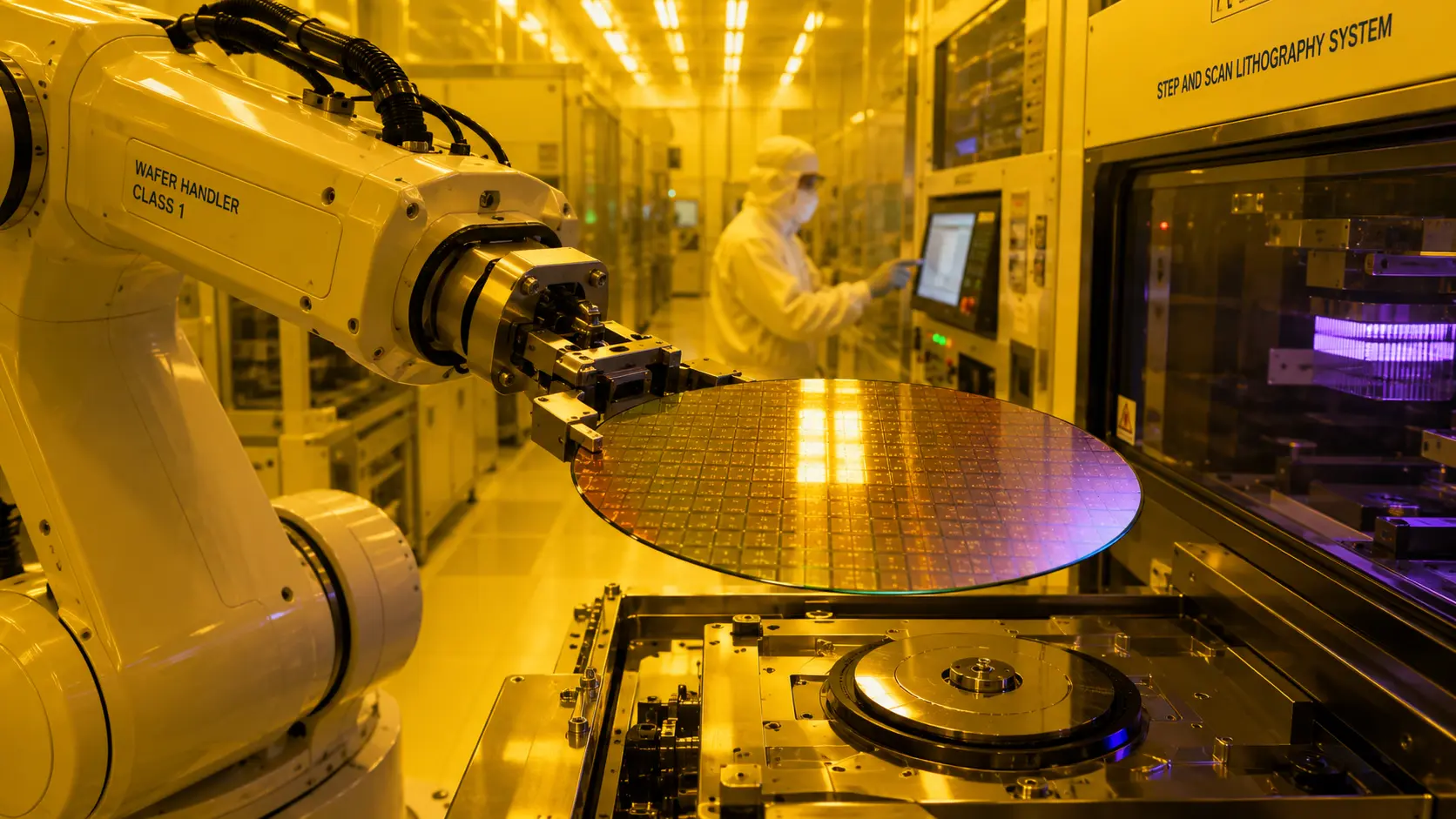
The manufacturing floor of a semiconductor fab behaves more like an advanced biochemical facility than a traditional factory. Photolithography—the process of printing microscopic nanoscale circuit architectures onto the wafer surface—requires specialized chemical layers known as photoresists.
Advanced Extreme Ultraviolet (EUV) and Deep Ultraviolet (DUV) photoresists stand among the world’s most guarded chemical formulations. India’s highly competitive commercial specialty chemical sector is uniquely positioned to bridge this gap. By upgrading standard chemical lines into highly sterile cleanrooms, local manufacturers can gradually move past basic industrial supplies into semiconductor-grade developers, anti-reflective coatings, and targeted cleaning solvents.
3. Shifting to 6N Purity: Semiconductor-Grade Gases
A single chip fab consumes massive volumes of process and ambient gases daily. While India maintains a mature industrial gas market, standard manufacturing demands are highly distinct from the stringent 6N (99.9999%) purity thresholds required inside a cleanroom.
[Standard Industrial Gas] (99.9%)──► [Advanced Refinement & Distillation]──► [Semiconductor-Grade Gas] (99.9999%)
                                                                                       │
    ┌──────────────────────────────┬──────────────────────────────┬────────────────────┴─────────────────────┐
    ▼                              ▼                              ▼                                          ▼
[Silane & Ammonia]           [Fluorinated Gases]         [Nitrogen & Argon]                       [Helium & Neon]
(Chemical Vapor Deposition)  (Plasma Etching Systems)    (Inert Cleanroom Environments)     (Laser Optics Systems
Sustaining this environment requires more than just local chemical purification; it demands highly certified specialty cylinder logistics, precise leak-proof distribution infrastructure, and continuous sub-parts-per-billion quality analysis at the fab boundary.
4. Lithography Support & Precision Mechatronics
Building an entire EUV or DUV lithography assembly domestically is a generational engineering task. However, Indian precision engineering firms are capturing a massive secondary market by integrating into the global components supply chain.
By scaling capabilities in high-performance lenses, ultra-flat sub-nanometer mirrors, vacuum sub-systems, and precision mechatronics, domestic players are supporting the global semiconductor equipment pipeline. Conveniently, these identical high-spec components serve as direct structural pillars for the nation’s expanding aerospace, satellite manufacturing, and advanced defense sectors.
5. Metrology & Testing Infrastructure: The Yield Engine
In semiconductor manufacturing, yield is everything. If a fab cannot consistently ensure that 85% to 95% of the microchips on a 300mm wafer are fully functional, the facility loses its global commercial viability.
To secure these high metrics, India is building out extensive regional metrology and failure-analysis clusters alongside its core production plants. Localizing deep electrical characterization, automated optical defect inspection, and specialized yield optimization software allows domestic facilities to catch manufacturing anomalies in real time without shipping sample wafers overseas for advanced testing.
6. Localizing the Substrate Layer in Advanced Packaging
Through heavy initial ATMP and OSAT investments, India has successfully anchored its presence in the downstream assembly market. However, the materials holding those packaged chips together—bonding wires, lead frames, underfill materials, and complex organic substrates—are still largely imported.
As traditional transistor scaling slows down, the global market is leaning into Advanced Packaging (stacking separate functional chiplets on top of one another). By localizing the production of high-density laminates, epoxy molding compounds, and advanced thermal interface materials, Indian packaging facilities can secure significantly higher local value addition per component.
7. Critical Minerals: The Geopolitical Supply Shield
A reliable semiconductor supply chain is completely tethered to the uninterrupted availability of rare earth elements and critical minerals like Gallium, Germanium, Indium, and high-purity graphite.
Because global supply networks for these minerals remain highly consolidated, India has deployed strategic policy counter-measures. This includes key structural pushes like the extended ₹7,280-crore Rare Earth Permanent Magnet (REPM) Scheme, which directly subsidizes the midstream processing capacity needed to turn raw oxide minerals into functional, high-grade components. Furthermore, bilateral treaties—such as the India-Australia Comprehensive Economic Cooperation Agreement (CECA)—guarantee reliable, long-term access to essential raw reserves like cobalt and lithium.
The Strategic Roadmap Ahead
India’s electronics and deep-tech ecosystem has successfully proved it can design world-class silicon architecture and construct state-of-the-art assembly facilities. The next decade belongs to the midstream and upstream material suppliers. By systematically localizing specialty chemical purification, wafer preparation, and critical mineral refining, India is actively transforming itself from an entry-level participant into a resilient, self-sufficient global superpower in the semiconductor space.
Frequently Asked Questions (FAQ)
Q1: Why can’t India use its local quartz reserves to make silicon wafers immediately?
While India possesses vast raw quartz deposits, transforming it into usable semiconductor wafers requires creating ultra-pure electronic-grade polysilicon (11N purity) and pulling flawless monocrystalline ingots. This demands multi-billion-dollar specialized purification infrastructure and highly specific manufacturing processes that the country is currently working to localize through global technology partnerships.
Q2: What is the main difference between standard industrial gases and semiconductor gases?
The core difference is the purity threshold. Standard heavy industries utilize gases at roughly 99.9% purity. Semiconductor fabrication cleanrooms require 6N purity (99.9999%) or higher. Even trace contamination of a few parts-per-trillion can cause widespread defects across a production wafer, ruining production yields.
Q3: How do schemes like the REPM initiative help India’s chip ecosystem?
The ₹7,280-crore Rare Earth Permanent Magnet (REPM) Scheme addresses the critical midstream gap. While India has access to raw rare earth deposits, it historically lacked the facilities to process them into high-grade magnets and components used in precision cleanroom robotics, automation motors, and advanced defense equipment. Localizing this processing protects the country from external supply blockades.
Q4: Why is packaging materials localization considered a “very high” priority?
India is building multiple ATMP/OSAT chip packaging plants. However, if these plants continue to import their internal substrates, lead frames, and molding compounds, the actual economic value added locally remains low. Localizing packaging materials ensures the country captures the most lucrative part of the backend manufacturing boom.
Disclaimer
The information presented in this article is intended solely for educational and informational purposes. Data, policy figures, and industry developments reflect the active market landscapes recorded as of July 2026. Readers seeking specific investment or commercial advice regarding the semiconductor manufacturing sector should consult certified industrial analysts and official policy briefs issued by the India Semiconductor Mission (ISM).
Relevant Links :
India Semiconductor Mission 2.0: The Rise of India’s High-Tech Microchip Manufacturing Ecosystem.
The Blueprint of Modern Tech: Mapping the Complete Electronics Manufacturing Supply Chain.
India’s Silicon Boom: Top Semiconductor Career Opportunities and How to Prepare.
India Australia CECA 2026: Ushering a New Era in Trade, Tech, and Green Energy.
