 Matribhumi Samachar English


Mumbai. Tuesday, 14 July 2026
The global artificial intelligence (AI) revolution is rewriting the rules of the tech industry, sparking an unprecedented semiconductor supercycle. At the very center of this massive transformation stands Taiwan Semiconductor Manufacturing Company (TSMC), operating as the primary engine for advanced AI hardware. As tech giants aggressively compete to construct next-generation data centers, generative AI platforms, and autonomous systems, the ripple effects are reshaping industrial capabilities worldwide. Crucially, this global boom is paving the way for emerging electronics manufacturing powerhouses, with India fast-tracking its ecosystem to anchor a resilient global supply chain.
The AI Engine Driving a $1.5 Trillion Supercycle
Artificial intelligence has evolved into the definitive growth catalyst for silicon technology. The global expansion of complex large language models (LLMs), enterprise automation, edge computing, and robotics requires vast computational power. Standard chips can no longer keep pace; instead, the market demands highly specialized Graphics Processing Units (GPUs) and bespoke AI accelerators.
Industry forecasters project that the global semiconductor market will surge past $1.5 trillion by 2030, with AI hardware infrastructure commanding the lion’s share of this valuation. To capture this momentum, leading foundries are pushing the absolute boundaries of physics, scaling sub-nanometer nodes like 3nm and upcoming 2nm architectures to maximize throughput while minimizing energy consumption.
Why TSMC Holds the Keys to the AI Kingdom
TSMC occupies a unique, highly strategic position in geopolitics and technology. Unlike companies that both design and market chips, TSMC operates strictly as a pure-play semiconductor foundry. It manufactures the physical silicon blueprints created by the world’s most dominant tech corporations.
TSMC’s elite roster of customers includes:
-
Nvidia & AMD: The creators of dominant AI training and inference processors.
-
Apple: Powering consumer-facing edge AI across billions of devices.
-
Qualcomm & Broadcom: Delivering essential connectivity, networking, and custom routing chips.
-
Hyperscale Cloud Providers: Tech giants building proprietary custom silicon internally.
Because these cutting-edge chips require ultra-advanced manufacturing capabilities, demand for TSMC’s capacity consistently outstrips global supply, resulting in record-breaking quarterly revenues and unmatched industry pricing leverage.
India’s Strategic Leap into the Silicon Value Chain
While leadingfoundries dominate advanced node fabrication, the global supply chain diversification push has opened massive windows of opportunity for South Asia. Through targeted state initiatives like the India Semiconductor Mission (ISM), India is systematically transforming itself from an intellectual hub for chip design into a physical manufacturing destination.
Rather than attempting to build multi-billion dollar leading-edge logic fabs overnight, India is executing a highly calculated, multi-tiered blueprint:
1. Capitalizing on World-Class Chip Design
India already hosts massive R&D centers for the world’s top technology firms. Thousands of indigenous engineers contribute to processor architecture, electronic design automation (EDA), and embedded system verification. Linking this design mastery with emerging localized fabrication creates an integrated, highly competitive footprint.
2. Accelerating with Advanced Packaging (ATMP / OSAT)
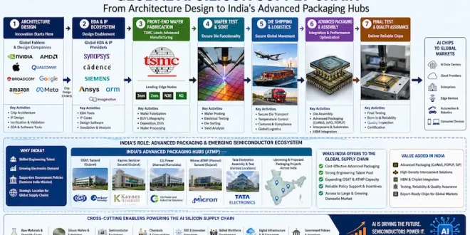
Advanced packaging—integrating distinct chiplets into one highly efficient computing module—is one of the fastest-accelerating sectors in silicon hardware. This is where India is securing its fastest commercial wins. Multi-billion dollar infrastructure deployments, such as Micron’s ATMP facility and Kaynes Semicon’s OSAT plant in Sanand, Gujarat, have transitioned seamlessly from policy approvals to active production lines.
3. Policy Scaling via ISM 2.0
Building upon primary manufacturing setups, the government is expanding its horizons via the updated ISM 2.0 framework. Backed by expanding pipelines—including major compound semiconductor fabs in Dholera and massive upcoming packaging facilities—this secondary policy wave aims to establish a self-sustaining local layer of semiconductor equipment, raw specialized materials, and dedicated deep-tech research infrastructure.
                GLOBAL AI SILICON PIPELINE
+---------------------------------------------------------+
|                Upstream Architecture                   |
|  Global Tech Giants & Indian Chip Design Engineers      |
+---------------------------------------------------------+
                            |
                            v
+---------------------------------------------------------+
|                  Front-End Fabrication                  |
|  TSMC Dominant Advanced Sub-5nm Nodes (Taiwan)          |
+---------------------------------------------------------+
                            |
                            v
+---------------------------------------------------------+
|                 Back-End Supply Chain                   |
|  India's Sanand & Dholera ATMP / OSAT Packaging Hubs    |
+---------------------------------------------------------+
Hurdles to Overcome on the Path to Self-Reliance
Despite immense policy momentum and strong financial incentives, building a mature semiconductor ecosystem requires overcoming notable structural bottlenecks:
-
Talent Pipelines: Cultivating a continuous, hyper-specialized local workforce trained in complex powder metallurgy, lithography, and cleanroom protocols.
-
Resource Infrastructure: Semiconductor facilities demand absolute stability—requiring uninterrupted power grids and millions of gallons of ultra-pure water daily.
-
Supply Chain Resilience: Minimizing global shocks by securing domestic critical minerals and specialized raw materials.
As the United States, Japan, and Europe deploy hundreds of billions in local subsidies to secure their own tech sovereignty, India’s strategy balances essential domestic self-reliance with vital international supply chain integration. By merging localized design talent, expanding packaging capacities, and robust policy updates, the global AI chip boom is actively serving as the ultimate catalyst for India’s emergence in the international technological hierarchy.
Key Takeaways for Global Tech Analysts
For an in-depth exploration of how regional tech policies and manufacturing ecosystems intersect with these global electronics supply chains, read the full analytical breakdown on India’s Electronics Manufacturing Boom: Engineering the Next Global Tech Superpower.
Additionally, understand how critical resource pipelines protect modern high-tech assembly lines by reviewing the policy details surrounding the India Extends ₹7280-Crore Rare Earth Permanent Magnet (REPM) Scheme Application Deadline.
Frequently Asked Questions (FAQ)
Q1: Why is TSMC so crucial to the generative AI revolution?
TSMC is the only foundry worldwide with the immediate commercial capacity, yield efficiency, and advanced sub-5nm lithography techniques required to physically manufacture the complex, high-density AI accelerators designed by companies like Nvidia and AMD.
Q2: What are ATMP and OSAT facilities, and why is India focusing on them?
ATMP stands for Assembly, Testing, Marking, and Packaging, while OSAT refers to Outsourced Semiconductor Assembly and Test. These facilities take raw silicon wafers, cut them, test them, and package them into final microchip modules. India is prioritizing this sector because it requires less initial capital expenditure than front-end mega-fabs while generating rapid job creation and supply chain value.
Q3: How does ISM 2.0 differ from the initial India Semiconductor Mission policy?
While the initial mission (ISM 1.0) succeeded in drawing in anchor manufacturing units and large-scale packaging plants, ISM 2.0 focuses heavily on building out the vital, secondary industrial layers—such as domestic chemical suppliers, specialized fabrication tools, design IP licensing, and targeted academic research partnerships.
Disclaimer: The information provided in this article is for educational and informational purposes only. The tech market analysis, corporate performance updates, and policy forecasts presented here are based on current industry evaluations and trends as of July 2026. Readers should consult specialized financial and industrial experts before making any related investment or corporate supply chain decisions.