 Matribhumi Samachar English


Mumbai. Thursday, 9 July 2026
The global semiconductor landscape is undergoing a massive transformation as technology companies diversify their supply chains. India has emerged as a premier destination for this expansion, evolving from a standalone design hub into a complete microchip ecosystem. Driven by the India Semiconductor Mission (ISM), massive multi-billion-dollar investments, and strategic global partnerships, the Indian semiconductor industry is entering an unprecedented phase of workforce demand.
For engineering graduates, experienced tech professionals, and students planning their career paths, the semiconductor boom offers stable, highly technical, and financially rewarding roles.
Why Semiconductor Careers Are Skyrocketing in India
Several structural factors are accelerating recruitment across the domestic electronics and chip manufacturing sectors:
-
Large-Scale Infrastructure Investments: Real physical fabrication units (fabs) and packaging plants are actively scaling up across the country.
-
Strategic Global Partnerships: Landmark corporate collaborations are bringing advanced technology and global standards directly to Indian soil. For instance, the Tata-ASML Partnership at Dholera is setting up India’s first commercial mega-fab.
-
The Rise of Sovereign Tech: The surging domestic need for AI accelerator hardware, electric vehicles (EVs), defense drones, and next-generation telecommunications requires localized silicon manufacturing to maintain strategic independence.
Top 6 High-Demand Semiconductor Job Roles
The semiconductor job market splits cleanly into software-based architecture (Upstream) and cleanroom-based physical production (Downstream).
1. Chip Design & VLSI Engineer
Design engineers write the logic and lay out the microscopic hardware architecture of integrated circuits.
-
Key Responsibilities: Digital/analog circuit design, RTL development, logic synthesis, and design verification.
-
Essential Skills: Verilog, SystemVerilog, VHDL, and industry-standard Electronic Design Automation (EDA) suites like Cadence and Synopsys.
2. Process Engineer
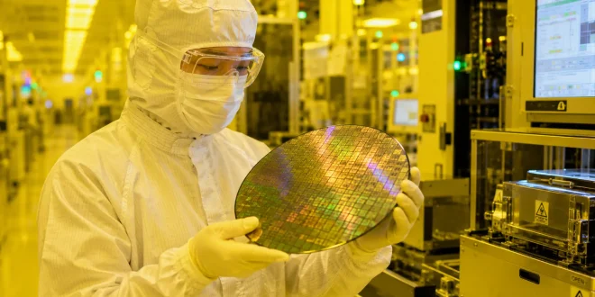
Process engineers operate inside state-of-the-art manufacturing facilities to monitor, scale, and optimize chemical and physical operations on silicon wafers.
-
Key Responsibilities: Managing lithography, thin-film deposition, plasma etching, and chemical processing.
-
Essential Skills: In-depth knowledge of cleanroom protocols, process integration, and material properties.
3. Packaging Engineer
As microchips shrink, advanced packaging technologies ensure multiple integrated components can communicate efficiently without overheating.
-
Key Responsibilities: Managing wire bonding, flip-chip assembly, thermal management, and reliability testing.
-
Essential Skills: Knowledge of chiplet architecture, microfluidic cooling, and structural testing.
4. Test & Yield Engineer
Before a physical chip is shipped to global clients, it must undergo thorough evaluation to catch manufacturing defects.
-
Key Responsibilities: Utilizing Automated Test Equipment (ATE), conducting root-cause failure analysis, and scaling up production efficiency.
-
Essential Skills: Statistical Process Control (SPC), data analytics, and failure mode mapping.
5. Equipment Engineer
Semiconductor fabrication plants utilize some of the most expensive and complex machinery on earth. Equipment engineers keep these intricate hardware setups operational.
-
Key Responsibilities: Tool calibration, preventative maintenance, and fault diagnosis.
-
Essential Skills: Advanced industrial automation, robotics, and electro-mechanical systems.
6. Quality & Reliability Engineer
These specialists guarantee that finished semiconductor products satisfy strict international tolerances and perform reliably over decades of use.
-
Key Responsibilities: Executing product quality audits, Six Sigma implementations, and environmental stress screening.
Educational Prerequisites & Technical Skillsets
Academic Backgrounds Preferred
Most domestic and multinational chip companies recruit candidates holding degrees in:
-
Electronics and Communication Engineering (ECE)
-
Electrical Engineering
-
Computer Engineering or Computer Science
-
Mechanical or Mechatronics Engineering (highly valued in equipment and packaging roles)
-
Materials Science or Physics
Note: While a Bachelor’s degree (B.Tech/B.E.) secures entry-level processing or testing roles, advanced research, core R&D, and premium design architecture positions typically look for an M.Tech or Ph.D. in VLSI, Microelectronics, or Nanotechnology.
Core Technical Toolsets to Master
To stand out to top-tier employers, aspiring semiconductor engineers should prioritize building a technical portfolio around these pillars:
-
Programming & Scripting: C, C++, Python, TCL, and Shell Scripting.
-
Hardware Description Languages (HDLs): Verilog, SystemVerilog, and VHDL.
-
Design & Simulation Software: Cadence Virtuoso, Synopsys Design Compiler, Siemens EDA, ANSYS, and COMSOL.
-
Hardware Interfacing: Field Programmable Gate Array (FPGA) development and embedded system design.
Typical Career Progression and Salary Outlook
The semiconductor space stands out as one of the highest-paying segments within the engineering domain. The global shortage of experienced chip-design and process talent gives specialized professionals an edge in career advancement.
| Experience Level | Typical Job Titles | Focus Areas |
| 0–2 Years | Graduate Engineer Trainee, Test Engineer, Associate Process Engineer | Foundational tool mastery, execution of basic test cases, cleanroom assistance. |
| 2–5 Years | Design Engineer, Verification Engineer, Equipment Engineer | Sub-system design ownership, independent fault diagnosis, process recipe optimization. |
| 5–10 Years | Senior Engineer, Technical Lead, Process Specialist | Architecture design, multi-team project coordination, handling vendor escalations. |
| 10+ Years | Principal Engineer, Engineering Manager, Technical Architect, R&D Head | Cross-functional strategic direction, technology roadmap definition, ecosystem scaling. |
Future Outlook: Emerging Horizons
The modern evolution of India’s tech landscape ensures that tomorrow’s careers will look far different than yesterday’s. Emerging segments like automotive electronics, GaN (Gallium Nitride) power devices for fast charging, and advanced silicon photonics are rapidly gaining traction.
Furthermore, this chip infrastructure acts as the foundational computing layer for adjacent high-tech developments. To understand how domestic chip production feeds straight into the broader national digital ecosystem, see how it serves as the foundational Silicon Backbone for India’s Sovereign AI Push. For students and active tech job seekers alike, mastering specialized semiconductor skills now offers a rare opportunity to enter a highly stable, high-value field just as its growth curve bends upward.
Frequently Asked Questions (FAQs)
1. Which engineering stream is best for a career in the semiconductor industry?
An educational background in Electronics and Communication Engineering (ECE) or Electrical Engineering offers the most direct path. However, Mechanical, Materials, and Computer Engineering graduates are also heavily recruited for equipment maintenance, materials analysis, and software tooling design.
2. Can fresh engineering graduates find direct employment in semiconductor fabs?
Yes. With the operationalization of new manufacturing facilities under the India Semiconductor Mission 2.0 framework, there is a rising demand for entry-level Graduate Engineer Trainees (GETs) in process control, automated testing, and cleanroom hardware tracking.
3. Why are programming skills like Python and C++ required for hardware/chip jobs?
Modern chip design relies closely on automated validation software. Engineers use Python and TCL scripts to automate thousands of simulation test cases, while C++ is essential for low-level embedded software verification and interacting with physical automated testing equipment.
4. What is the difference between working in chip design versus a chip fab?
Chip design is software-centric and involves creating logical layouts and architectural definitions on workstations using specialized EDA tools. Working in a fabrication plant (fab) involves managing the physical, cleanroom-bound manufacturing machinery, managing chemical processing, and physically executing chip wafer layers.
Disclaimer
The career advice, salary trends, and skill requirements outlined in this article are collected from prevailing market reports and structural semiconductor sector data. Actual hiring timelines, compensation structures, and individual eligibility criteria vary based on specific corporate recruitment policies, institutional qualifications, and evolving industry market conditions.