

Mumbai. Monday, 20 July 2026
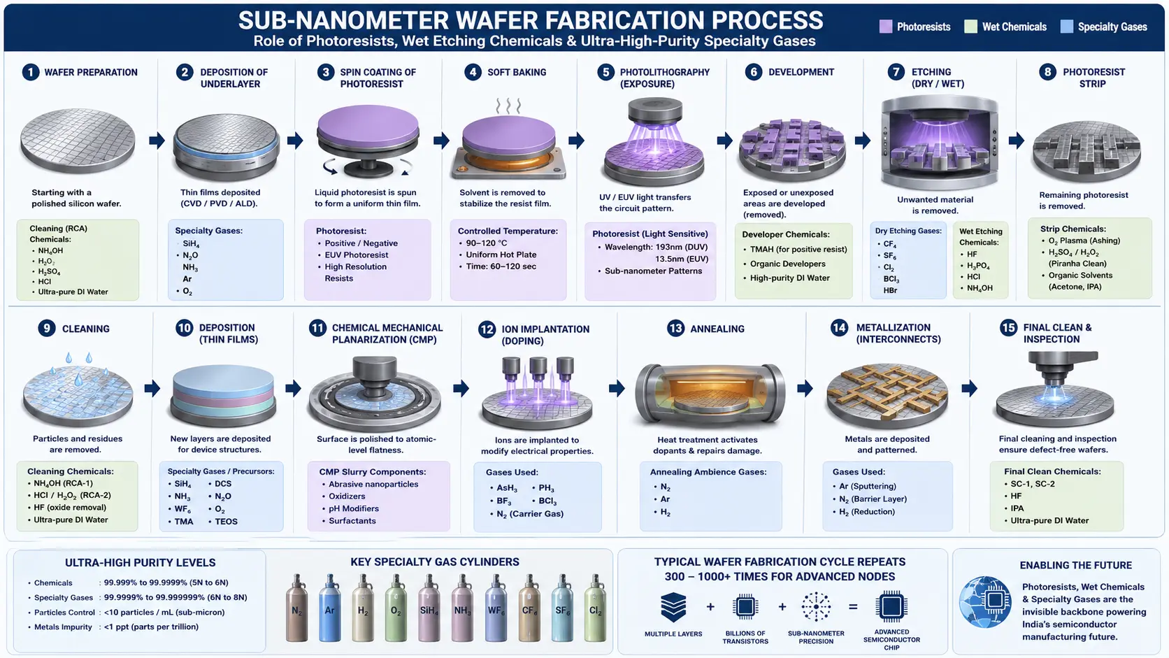
While mega-fabrication units (fabs) and multi-billion-dollar cleanrooms dominate headlines, the semiconductor industry’s success relies equally on an advanced upstream ecosystem: semiconductor chemicals and specialty gases. Every single silicon wafer undergoes hundreds of precision processing steps involving ultra-high-purity (UHP) materials that enable chip fabrication with nanometer accuracy.
As India accelerates investments in semiconductor manufacturing under the expanded India Semiconductor Mission (ISM) framework, building a local supply chain for semiconductor-grade chemicals and specialty gases has evolved into a strategic national priority.
What Are Semiconductor Chemicals?
Semiconductor chemicals are ultra-high-purity liquid and gaseous compounds used throughout the wafer fabrication process. Because microscopic impurities at the parts-per-billion or parts-per-trillion level cause fatal chip defects, purity levels of 99.9999% (6N) for wet chemicals and 99.999999% (8N) for specialty gases are mandatory.
The critical categories driving modern microchip fabrication include:
                  ┌─────────────────────────────────────────┐
                  │    Semiconductor Chemical Ecosystem    │
                  └────────────────────┬────────────────────┘
                                       │
      ┌─────────────────┬──────────────┼──────────────┬─────────────────┐
      │                 │              │              │                 │
┌─────┴──────┐   ┌──────┴──────┐  ┌────┴─────┐  ┌─────┴──────┐   ┌──────┴──────┐
│Photoresists│   │ CMP Slurries│  │ UHP Gases│  │ Wet Chem/  │   │ Deposition  │
│  & EUV     │   │ & Polishing │  │ & Etchants│ │ Cleaning   │   │ Precursors  │
└────────────┘   └─────────────┘  └──────────┘  └────────────┘   └─────────────┘
1. Photoresists: transferred nanoscale circuit patterns
Photoresists are light-sensitive polymers used during photolithography to transfer circuit patterns onto silicon wafers.
Types of Photoresists
Positive Photoresists: Exposed regions dissolve during development. They are the preferred option for advanced semiconductor nodes due to high resolution.
Negative Photoresists: Exposed regions cross-link and harden. Primarily used in MEMS, sensors, and legacy packaging.
Advanced EUV Photoresists: Formulated specifically for Extreme Ultraviolet (EUV) photolithography at 7nm, 5nm, 3nm, and upcoming 2nm nodes.
Applications & Manufacturing Challenges
Photoresists are required across logic chips, memory devices, CMOS image sensors, MEMS, and power semiconductors. Creating them requires molecular-scale precision, near-zero metallic contamination, controlled viscosity, long shelf life, and uniform coating capabilities.
2. CMP Slurries: Achieving Atomic-Level Flatness
Chemical Mechanical Planarization (CMP) slurries smooth and polish wafer surfaces between successive layer deposition steps. By combining chemical etching with mechanical abrasive polishing, CMP delivers the atomic-level surface flatness required for complex multi-layer chips (which can demand 20–40 individual CMP steps).
CMP Slurry Components & Substrates
Components: Nano-sized abrasive particles, oxidizers, corrosion inhibitors, surfactants, and pH modifiers.
Target Materials: Applied directly on silicon, copper, tungsten, oxides, and low-k dielectrics.
3. Ultra-High Purity (UHP) Specialty Gases
Semiconductor cleanrooms consume high volumes of specialty gases every day, with purity thresholds exceeding 99.999999% (8N).
| Gas Name | Formula | Primary Fab Application |
| Nitrogen | $\text{N}_2$ | Cleanroom purging and dry environment maintenance |
| Argon | $\text{Ar}$ | Sputtering and plasma processes |
| Hydrogen / Oxygen | $\text{H}_2 / \text{O}_2$ | Thermal oxidation, surface reduction, and annealing |
| Helium | $\text{He}$ | In-process wafer cooling and leak detection |
| Silane / DCS | $\text{SiH}_4 / \text{SiH}_2\text{Cl}_2$ | Silicon layer deposition and epitaxy |
| Tungsten Hexafluoride | $\text{WF}_6$ | Tungsten interconnect deposition |
| Phosphine / Arsine | $\text{PH}_3 / \text{AsH}_3$ | N-type wafer doping |
| Fluorinated Gases | $\text{CF}_4, \text{SF}_6, \text{NF}_3$ | Plasma etching and chamber cleaning |
4. Wet Chemicals, Etchants, and Cleaning Solutions
Wafer cleaning accounts for a substantial percentage of all semiconductor processing steps to remove organic contaminants, metal ions, native oxides, and photoresist residues.
Essential Wet Chemicals
Hydrofluoric Acid ($\text{HF}$): Primary agent for native oxide removal and wet etching.
Sulfuric Acid ($\text{H}_2\text{SO}_4$) & Hydrogen Peroxide ($\text{H}_2\text{O}_2$): Used in Piranha cleaning mixtures to strip organic contaminants.
RCA Cleaning Standards: RCA-1 ($\text{NH}_4\text{OH} + \text{H}_2\text{O}_2$) for organic/particle removal; RCA-2 ($\text{HCl} + \text{H}_2\text{O}_2$) for metallic trace removal.
Solvents: Electronic-grade Isopropyl Alcohol ($\text{IPA}$) for spot-free drying and Acetone for photoresist stripping.
India’s Semiconductor Chemical Opportunity
As commercial fabs and OSAT facilities scale up across India under the India Semiconductor Mission, establishing localized chemical capabilities is moving from an operational advantage to a national strategy.
Primary Opportunity Areas
Electronic-Grade Acids & Solvents: Manufacturing UHP sulfuric, nitric, and hydrofluoric acids locally.
Gas Infrastructure: Developing local gas purification plants, bulk storage systems, and specialized gas cabinets.
Consumables & Recycling: CMP slurry blending and chemical waste treatment/recycling plants.
Key Strategic Challenges
Achieving 6N–8N Purity: Establishing ultra-clean distillation and testing facilities capable of zero-ppm contamination.
Fab Qualification Cycles: Global chipmakers require 1 to 3 years of rigorous testing before approving new chemical suppliers.
Hazardous Materials Logistics: Transporting hazardous materials like Arsine ($\text{AsH}_3$) or Silane ($\text{SiH}_4$) safely across regions.
Related Coverage on Matribhumi Samachar
For further reading on India’s deep-tech manufacturing expansion and supply chain initiatives:
Read about the physical manufacturing rollout in India Semiconductor Mission 2.0: The Rise of India’s High-Tech Microchip Manufacturing Ecosystem.
Explore critical mineral supply chains in India Australia CECA 2026: Ushering a New Era in Trade, Tech, and Green Energy.
Learn about local raw material strategies in the India Extends ₹7,280-Crore Rare Earth Permanent Magnet Scheme.
Frequently Asked Questions (FAQ)
Q1: Why is 99.9999% (6N) purity required for semiconductor chemicals?
At the nanometer scale (e.g., 3nm or 5nm), even a single foreign metallic ion or microscopic particle can break a circuit line, causing wafer defects or total chip failure.
Q2: What is the difference between positive and negative photoresists?
Positive photoresists become soluble when exposed to light and are used for high-precision advanced nodes. Negative photoresists harden when exposed to light and are typically used for wider feature sizes in packaging, sensors, and MEMS.
Q3: Why are CMP slurries necessary in multi-layer chip fabrication?
Modern processors consist of dozens of stacked copper and silicon layers. CMP slurries polish each layer flat to provide a smooth base for subsequent photolithography and material deposition.
Q4: How does domestic chemical production support the India Semiconductor Mission (ISM)?
Localizing chemical and gas manufacturing cuts import dependence, shields domestic fabs from geopolitical supply shocks, lowers logistics costs, and speeds up fab qualification pipelines.
Disclaimer: This article is intended strictly for educational and informational purposes. Technical specifications, chemical classifications, and industrial policy references under the India Semiconductor Mission (ISM) reflect industry data and public notifications available as of July 2026.
